
Page 151 - Engineering Digital Design
P. 151
122 CHAPTER 3 / BACKGROUND FOR DIGITAL DESIGN
A B Y A B Y A B Y A B Y A B Y
LV LV HV LV LV LV LV LV LV LV LV HV LV LV LV
LV HV HV LV HV HV LV HV LV LV HV LV LV HV HV
HV LV HV HV LV HV HV LV LV HV LV LV HV LV HV
HV HV LV HV HV HV HV HV HV HV HV LV HV HV LV
(a) (b) (c) (d) (e)
FIGURE P3.1
3.3 By using a sketch, indicate how the CMOS inverter of Fig. 3.6a can be converted to a
two-transistor noninverting switch. What would be the disadvantage (if any) of such
a device?
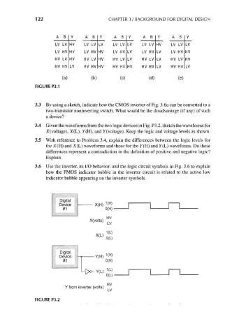
3.4 Given the waveforms from the two logic devices in Fig. P3.2, sketch the waveforms for
X(voltage), X(L), F(H), and 7 (voltage). Keep the logic and voltage levels as shown.
3.5 With reference to Problem 3.4, explain the differences between the logic levels for
the X(H) and X(L) waveforms and those for the Y(H) and Y(L) waveforms. Do these
differences represent a contradiction in the definition of positive and negative logic?
Explain.
3.6 Use the inverter, its I/O behavior, and the logic circuit symbols in Fig. 3.6 to explain
how the PMOS indicator bubble in the inverter circuit is related to the active low
indicator bubble appearing on the inverter symbols.
Digital
Device y/u\ 1(H)
A^n;
#1 0(H)
HU
X(volts) •• •
Digital
Device f Y(H) '^
#2 0(H)
HV
Y from inverter (volts)
FIGURE P3.2