
Page 146 - Engineering Digital Design
P. 146
Digital
Device r-0»-| — X(Volts) LV Given
1
-X(H)
0
Lx(L) 1 Answer
0
Digital 1 Given
Device X(H) 0
1
1 X(L)
0 Required
HV Answer
X(Volts)
LV
(b)
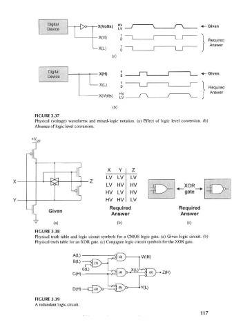
FIGURE 3.37
Physical (voltage) waveforms and mixed-logic notation, (a) Effect of logic level conversion, (b)
Absence of logic level conversion.
X Y Z
LV LV LV
HV
LV HV HV o
H HV LV gate 4 >
Y HV HV LV
Required Required
Given
Answer Answer
T (a) (b) (c)
FIGURE 3.38
Physical truth table and logic circuit symbols for a CMOS logic gate, (a) Given logic circuit, (b)
Physical truth table for an XOR gate, (c) Conjugate logic circuit symbols for the XOR gate.
W(H)
_^ Z(H)
Y(L)
r
— \- -/ ' i * s ~ ~i ^^
FIGURE 3.39
A redundant logic circuit.
117