
Page 145 - Engineering Digital Design
P. 145
116 CHAPTER 3 / BACKGROUND FOR DIGITAL DESIGN
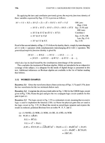
By applying the laws and corollaries previously given, the majority functions identity of
three variables expressed by Eqs. (3.33) is proven as follows:
XY + YZ + XZ = XY(Z + Z) + (X + X)YZ + X(Y + F)Z OR Laws
[Eqs. (3.8)]
= XYZ + XYZ + XYZ + XYZ + XYZ + XYZ Eqs. (3.19) and
OR Laws
= XYZ © XYZ © (XYZ + XYZ) Corollary I
= XY®(Y®X}Z Eqs. (3.19), OR
Law, Eq. (3.4)
= XY®YZ®XZ. Eq. (3.8)
Proof of the second identity of Eqs. (3.33) follows by duality, that is, simply by interchanging
all (+) with (•) operators while simultaneously interchanging all © with O operators. The
generalized majority function identity is given by
[WXY ••• + WXZ ••• + WYZ • • • + XYZ ...+ ...]
= [WXY • • • © WXZ • • • © WYZ • • • © XYZ •••©•••] ,
which also has its dual formed by the simultaneous interchange of the operators.
This concludes the treatment of Boolean algebra. While not intended to be an exhaustive
coverage of the subject, it is adequate for the needs of digital design as presented in this
text. Additional references on Boolean algebra are available in the list of further reading
that follows.
3.12 WORKED EXAMPLES
EXAMPLE 3.1 Given the waveforms (heavy lines) at the top of Figs. 3.37a and 3.37b, draw
the two waveforms for the two terminals below each.
EXAMPLE 3.2 Complete the physical truth table in Fig. 3.38b for the CMOS logic circuit
given in Fig. 3.38a. Name the gate and give the two conjugate logic circuit symbols for this
gate in part (c).
EXAMPLE 3.3 The logic circuit in Fig. 3.39 is a redundant circuit, meaning that excessive
logic is used to implement the function Z(H). (a) Name the physical gates that are used in
the logic circuit in Fig. 3.39. (b) Read the circuit in mixed-logic notation and express the
results in reduced, polarized Boolean form at nodes W, X, Y, and Z.
(a) (1) NAND, (2) NOR, (3) NOR, (4) OR, (5) AND, (6) NOR
(b) W(H) = AB(H)
X(L)= BC(L)
Z(H) = WXY(H) = (AB)(BC)(C + D)(//) = (A + B}(BC}(C + D)(H)
= (A + B)(BC + BCD)(H)
= ABC(H)