Page 184 - Engineering Digital Design
P. 184

4.5 MULTIPLE OUTPUT OPTIMIZATION                                     155


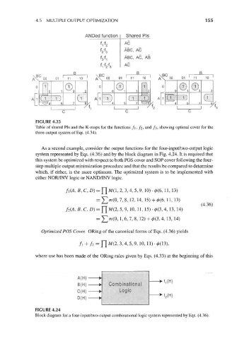
                                      ANDed function  Shared Pis
                                                     AC
                                            fl*2
                                                     ABC, AC
                                            f 2'f 3
                                                     ABC, AC, AB
                                            ¥l
                                                     AC
                                            M 2 *3
                  BC         i   B    1   \BC         i   B    1   \BC         i   B    1
                 \ 00     01  11   10     A\ °°    01  11   10    A \ °°   01   11   10
                  o [7                     0    0 ©,        IT)     0
                       0    1 ©3     2                    3    2         0 ©, ©3        2
                                          I —
                  1 Q_   1 }      (i                   rr~   1 )      ( 1    1)      (1
                   -^=3 4   5   7    6 /  A^T)  4    5    7  t=Tg        4    5    7    6
                                                              /T                        /
                                     A                          2
                 FIGURE 4.23
                 Table of shared Pis and the K-maps for the functions f\, fa, and /3, showing optimal cover for the
                 three-output system of Eqs. (4.34).


                    As a second example, consider the output functions for the four-input/two-output logic
                 system represented by Eqs. (4.36) and by the block diagram in Fig. 4.24. It is required that
                 this system be optimized with respect to both POS cover and SOP cover following the four-
                 step multiple output minimization procedure and that the results be compared to determine
                 which, if either, is the more optimum. The optimized system is to be implemented with
                 either NOR/INV logic or NAND/INV logic.

                              /i (A, B,C, D) =  M(l,2, 3,4, 5,9, 10) • 0(6, 11,13)
                                              k
                                          = V m(0, 7, 8, 12, 14, 15) + 0(6, 11, 13)
                                            T^                                       (4.36)
                              / 2(A, fi,C, D) = JJM(2, 5,9, 10, 11, 15) • 0(3, 4, 13, 14)
                                                      6  7  8  12
                                                                 3
                                                 (°> 1» > - ' > + <K > 4, 13, 14)
                    Optimized POS Cover. ORing of the canonical forms of Eqs. (4.36) yields
                                               M(2 3 4 5 9 io  1 1} (13)
                                   /i + h = n ' ' ' ' ' '  • ^ '


                 where use has been made of the ORing rules given by Eqs. (4.33) at the beginning of this


                                  A(H)     >
                                  B(H)     >   Combinational
                                  C(H)    >        Logic
                                  D(H)     >

                 FIGURE 4.24
                 Block diagram for a four-input/two-output combinational logic system represented by Eqs. (4.36).
   179   180   181   182   183   184   185   186   187   188   189