
Page 152 - High Power Laser Handbook
P. 152
120 Diode Lasers Semiconductor Laser Diodes 121
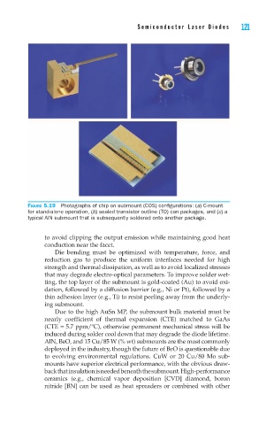
Figure 5.19 Photographs of chip on submount (COS) configurations: (a) C-mount
for stand-alone operation, (b) sealed transistor outline (TO) can packages, and (c) a
typical AlN submount that is subsequently soldered onto another package.
to avoid clipping the output emission while maintaining good heat
conduction near the facet.
Die bonding must be optimized with temperature, force, and
reduction gas to produce the uniform interfaces needed for high
strength and thermal dissipation, as well as to avoid localized stresses
that may degrade electro-optical parameters. To improve solder wet-
ting, the top layer of the submount is gold-coated (Au) to avoid oxi-
dation, followed by a diffusion barrier (e.g., Ni or Pt), followed by a
thin adhesion layer (e.g., Ti) to resist peeling away from the underly-
ing submount.
Due to the high AuSn MP, the submount bulk material must be
nearly coefficient of thermal expansion (CTE) matched to GaAs
(CTE = 5.7 ppm/ºC), otherwise permanent mechanical stress will be
induced during solder cool down that may degrade the diode lifetime.
AlN, BeO, and 15 Cu/85 W (% wt) submounts are the most commonly
deployed in the industry, though the future of BeO is questionable due
to evolving environmental regulations. CuW or 20 Cu/80 Mo sub-
mounts have superior electrical performance, with the obvious draw-
back that insulation is needed beneath the submount. High-performance
ceramics (e.g., chemical vapor deposition [CVD] diamond, boron
nitride [BN] can be used as heat spreaders or combined with other