Page 151 - High Power Laser Handbook
P. 151
120    Diode Lasers                                                                                                      Semiconductor Laser Diodes    121


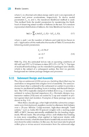
                      where E  is a thermal activation energy and m and n are exponents of
                             a
                      current  and  power  accelerations,  respectively.  To  derive  model
                      parameters E , m, and n, the maximum likelihood method is used.
                                 a
                      This method finds the model parameters by maximizing the likeli-
                      hood of observing actual number of failures on the test. For a random
                      exponential distribution of failures, the time likelihood function L is

                                       cellls
                                                 ,, )) − ∑
                                              λ
                                                             IP
                                   ln()L =  n i  ln((TI i  P i  λ  (T ji , ,)t      (5.7)
                                                                 i
                                                ji
                                                                i
                                                             i
                                        i
                      where n  and t  are the number of failures and total device hours in
                             i
                                  i
                      cell i. Application of this method to the results of Table 5.2 extracts the
                      following model parameters:
                                                 .
                                             E = 078  eV
                                              a
                                              m = 27.                       (5.8)
                                             n = 0
                      With Eq. (5.6), the estimated failure rate at operating conditions of
                                                                     –1
                                                                  –9
                      400 mW and 25ºC is 53 failures-in-time (FIT) (53 × 10  hr ). This type
                      of multicell methodology can be extended to packaged laser diodes,
                      which  is  the  subject  of  a  subsequent  section.  But  first  we  provide
                      background on various package designs and processes.
                 5.11  Submount Design and Assembly
                      The chip-on-submount (COS) serves as a building block that may be
                      used alone or integrated into a higher level of assembly. The semicon-
                      ductor laser chip is soldered to the submount (or carrier) to provide a
                      means for mechanical handling, burn-in testing, and thermal dissipa-
                      tion. The COS is typically clamped or bolted down (e.g., C-mount) or
                      soldered to reduce thermal impedance (R ). Hermetic designs (e.g.,
                                                         th
                      transistor outline [TO] cans) are sealed by a cap and window to pro-
                      tect against dust and moisture. Examples of these package types are
                      shown in Fig. 5.19.
                         More than a decade ago, when high-reliability submarine compo-
                      nents were first deployed, suppliers needed to eliminate field failures
                      over  a  25-year  lifetime.  Creep-resistant,  high-shear-strength  “hard
                      solders,” such as AuSn (80/20 percent weight) with a melting point
                      (MP) of 280ºC, became universally established for die bonding single-
                      mode, 980-nm lasers. The advantage of flux- and whisker-free bonding
                      is  even  more  compelling  when  applied  to  high-power  diodes  with
                      p-side-down bonds, where the laser facet is located only several microm-
                      eters from the solder interface. In this case, the facet must also be placed
                      within plus or minus several micrometers from the submount edge

