
Page 204 - Introduction to Information Optics
P. 204
3.3. Critical Components 189
-AAAAA-* <—O hole
electro^
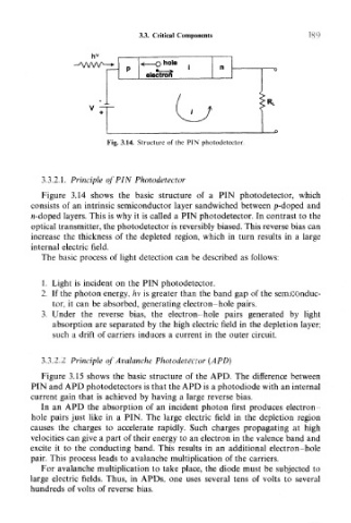
Fig. 3.14. Structure of the PIN photodetector.
3.3.2.1. Principle of PIN Photodetector
Figure 3.14 shows the basic structure of a PIN photodetector, which
consists of an intrinsic semiconductor layer sandwiched between p-doped and
n-doped layers. This is why it is called a PIN photodetector. In contrast to the
optical transmitter, the photodetector is reversibly biased. This reverse bias can
increase the thickness of the depleted region, which in turn results in a large
internal electric field.
The basic process of light detection can be described as follows:
1. Light is incident on the PIN photodetector.
2. If the photon energy, hv is greater than the band gap of the semiconduc-
tor, it can be absorbed, generating electron-hole pairs.
3. Under the reverse bias, the electron-hole pairs generated by light
absorption are separated by the high electric field in the depletion layer;
such a drift of carriers induces a current in the outer circuit.
3.3.2.2. Principle of Avalanche Photodetector (API)}
Figure 3.15 shows the basic structure of the APD. The difference between
PIN and APD photodetectors is that the APD is a photodiode with an internal
current gain that is achieved by having a large reverse bias.
In an APD the absorption of an incident photon first produces electron
hole pairs just like in a PIN. The large electric field in the depletion region
causes the charges to accelerate rapidly. Such charges propagating at high
velocities can give a part of their energy to an electron in the valence band and
excite it to the conducting band. This results in an additional electron-hole
pair. This process leads to avalanche multiplication of the carriers.
For avalanche multiplication to take place, the diode must be subjected to
large electric fields. Thus, in APDs, one uses several tens of volts to several
hundreds of volts of reverse bias.