
Page 329 - System on Package_ Miniaturization of the Entire System
P. 329
Radio Fr equency System-on-Package (RF SOP) 303
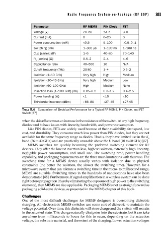
Parameter RF MEMS PIN Diode FET
Voltage (V) 20–80 ±3–5 3–5
Current (mA) 0 0–20 0
Power consumption (mW) <0.5 5–100 –0.5–0. 1
Switching time 1–300 μs 1–100 ns 1–100 ns
Cup (series) (fF) 1–6 40–80 70–140
R (series) (Ω) 0.5–2 2–4 4–6
s
Capacitance ratio 40–500 10 N/A
Cutoff frequency (THz) 20-80 1–4 0.5–2
Isolation (1 –10 GHz) Very high High Medium
Isolation (10–40 GHz) Very high Medium Low
Isolation (60–100 GHz) High Medium None
Insertion loss (1–100 GHz) (dB) 0.05–0.2 0.3–1.2 0.4–2.5
Power handing (W) <1 <10 <10
Third-order intercept (dBm) +66–80 +27–45 +27-45
TABLE 5.4 Comparison of Electrical Performance for a Typical RF MEMS, PIN Diode, and FET
Switch [67]
when the skin effect causes an increase in the resistance of the switch. At any high frequency,
diodes tend to have issues with linearity, bandwidth, and power consumption.
Like PIN diodes, FETs are widely used because of their availability, fast speed, low
cost, and durability. They consume much less power than PIN diodes, but they are not
available for the same frequency range as diodes. That is, they have limited use in the K a
band (26 to 40 GHz) and are practically unusable above the U band (40 to 60 GHz) [67].
MEMS switches are quickly becoming the preferred switching element for RF
devices. They offer the lowest insertion loss, highest isolation, extremely high linearity,
negligible power consumption, and small size. The switching time, power handling
capability, and packaging requirements are the three main limitations with their use. The
switching time for a MEMS device usually varies with isolation due to physical
constraints (the better the isolation, the slower the switching time). However, for a
microwave system that can tolerate a switching time in the micro- to millisecond range,
MEMS are suitable. Switching times in the hundreds of nanoseconds have also been
demonstrated [68]. Furthermore, if signal amplification in a wireless system can be done
right before propagation (thereby eliminating the exposure of high power to the switching
elements), then MEMS are also applicable. Packaging MEMS is not as straightforward as
packaging solid-state devices, as presented in the MEMS chapter of this book.
Challenges
One of the most difficult challenges for MEMS designers is overcoming dielectric
charging. All electrostatic MEMS switches use some sort of dielectric to maintain the
voltage potential. Over time, this dielectric will store charge and the switch will remain
in the actuated state. This charge naturally dissipates into the substrate, but it can take
anywhere from milliseconds to hours for this to occur, depending on the actuation
voltage, the substrate material, and the extent of the charging. Lower actuation voltages