
Page 327 - System on Package_ Miniaturization of the Entire System
P. 327
Radio Fr equency System-on-Package (RF SOP) 301
Operating Principle
RF MEMS switches are one type of MEMS device that utilize either a single-supported
(cantilever) or double-supported (air-bridge) beam suspended over a metal pad. Since
a MEMS switch uses only a single moving part, it is one of the simplest devices in use
today. By comparison, a typical sensor can have dozens of moving parts. Switches come
in a variety of shapes, sizes, and materials. There are two main types of actuation
mechanisms for RF MEMS switches: thermal and electrostatic.
Most materials expand when heated and contract when cooled. This is the basic
principle behind thermal switches that use a resistive material on the switch membrane.
When electric current is passed through the switch, the resistive material heats up,
causing it to expand. This expansion deflects the beam. When the current is reduced (or
eliminated), the switch returns to the steady state. This type of switch is not widely
used because it is much slower, lossier, has a lower bandwidth, consumes more power,
and is more difficult to control than electrostatic actuation. It can have a low actuation
voltage, however, which could make it attractive for system-on-chip applications.
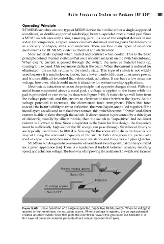
Electrostatic actuation relies on the principle that opposite charges attract. With one
metal beam suspended above a metal pad, a voltage is applied to the beam while the
pad is grounded or vice versa (as shown in Figure 5.40). A static charge will form from
the voltage potential, and this creates an electrostatic force between the layers. As the
voltage potential is increased, the electrostatic force strengthens. When this force
exceeds the beam’s ability to resist deflection, the metal layers are pulled together. If the
metal layers are allowed to make direct contact, this switch becomes “ohmic” and direct
current is able to flow through the switch. If direct contact is prevented by a thin layer
of dielectric, usually by silicon nitride, then the switch is “capacitive” and no direct
current is allowed to flow. Since a capacitor is the basis for this design, the frequency
must be sufficiently high so that the RF energy can pass through. Switches of this type
are typically used from 5 to 100 GHz. Varying the thickness of the dielectric layer is one
way of tuning the resonant frequency of the switch. Filter designers are particularly
fond of capacitive switches since there is no resistance and this gives a higher Q factor.
MEMS switch designers have a number of variables at their disposal that can be optimized
for a given application [66]. There is a fundamental tradeoff between isolation, switching
speed, and actuation voltage. The best way of improving the isolation of a switch is to increase
Positive voltage applied
Switch ON
Dielectric
No voltage applied
Switch OFF
FIGURE 5.40 Basic operation of a single-supported, capacitive MEMS switch. When no voltage is
applied to the membrane, no actuation occurs. When a voltage is applied, the voltage potential
creates an electrostatic force that pulls the membrane toward the grounded line beneath it. A
thin layer of dielectric material prevents direct contact between the layers.