
Page 322 - System on Package_ Miniaturization of the Entire System
P. 322
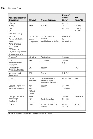
296    Cha pte r  F i v e


                                                                      Range of
                Name of Company or                                    Values      TCR
                                                                                       o
                Organization        Material    Process Approach      (Ω/sq)      (ppm/ C)
                Intarsia                                              10–100
                Boeing              Ta2N        Sputter               20           (±100)
                NTT                                                   25–125       (–75 to
                GE                                                                –100)
                Osaka University
                Metech              Conductive  Polymer thick-film    Insulating
                Acheson Colloids    polymer     process               to
                Electra             composites  Liquid phase sintering  conducting
                Ashai Chemical
                W. R. Grace
                DOW Corning
                Raychem Corporation
                Ormet Corporation
                Ohmega Ply          NiP alloy   Electroplate          25–500
                 Inst.              TaSi        DC sputter            10–40
                Microelectronics,                                     8–20
                Singapore
                University of       CrSi        Sputter                           –40
                Arkansas/Sheldahl
                W. L. Gore and      TiW         Sputter               2.4–3.2
                Associates
                Shipley             Doped Pt    Plasma enhanced       Up to 1000  100
                                    on Cu foil  chemical vapor
                                                deposition (PECVD)
                Deutsche Aerospace  NiCr        Sputter               35–100
                TICER Technologies  NiCr                              25–1000
                                    NiCrAlSi
                                    CrSiO3
                Georgia Institute of   NiWP                           10–50       Near zero
                Technology          NiP         Electroless plate     25–100
                MacDermid
                DuPont              LaB6        Screen print and foil   Up to     ±200
                                                transfer              10,000


               TABLE 5.3  Current State-of-the-Art of Embedded Resistors