
Page 321 - System on Package_ Miniaturization of the Entire System
P. 321
Radio Fr equency System-on-Package (RF SOP) 295
foil have received much attention. However, low TCR (<100 ppm/°C) and high
tolerance (<5 percent) have not been achieved. Tolerances on the order of 1 to 2 percent
are required for analog applications but cannot be achieved without the added cost of
laser trimming. Table 5.3 shows the current state-of-the-art in embedded resistors. In
most technologies presented in the table, the process tolerances are around 10 to 15 percent
without trimming.
5.4.7 Filters
Filters are essential components in many communication systems as they perform the
important tasks of channel selection (or rejection) and signal separation. There are three
filter technologies available using ceramics, silicon, and organics. Each of these
technologies can be used either as discrete components (IPDs) that are surface bonded
or as embedded components in the substrate, both as discretes or as thin-film layers.
In-package embedded or integrated multilayer filters offer a more attractive implementation
than on-chip and discrete filters. The design of filters and their implementation in
organic substrates have been explained in detail in Chapter 4. In this section, filters
implemented using LTCC and SOP processes are discussed.
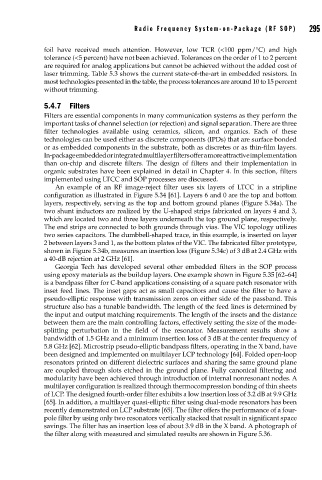
An example of an RF image-reject filter uses six layers of LTCC in a stripline
configuration as illustrated in Figure 5.34 [61]. Layers 6 and 0 are the top and bottom
layers, respectively, serving as the top and bottom ground planes (Figure 5.34a). The
two shunt inductors are realized by the U-shaped strips fabricated on layers 4 and 3,
which are located two and three layers underneath the top ground plane, respectively.
The end strips are connected to both grounds through vias. The VIC topology utilizes
two series capacitors. The dumbbell-shaped trace, in this example, is inserted on layer
2 between layers 3 and 1, as the bottom plates of the VIC. The fabricated filter prototype,
shown in Figure 5.34b, measures an insertion loss (Figure 5.34c) of 3 dB at 2.4 GHz with
a 40-dB rejection at 2 GHz [61].
Georgia Tech has developed several other embedded filters in the SOP process
using epoxy materials as the buildup layers. One example shown in Figure 5.35 [62–64]
is a bandpass filter for C-band applications consisting of a square patch resonator with
inset feed lines. The inset gaps act as small capacitors and cause the filter to have a
pseudo-elliptic response with transmission zeros on either side of the passband. This
structure also has a tunable bandwidth. The length of the feed lines is determined by
the input and output matching requirements. The length of the insets and the distance
between them are the main controlling factors, effectively setting the size of the mode-
splitting perturbation in the field of the resonator. Measurement results show a
bandwidth of 1.5 GHz and a minimum insertion loss of 3 dB at the center frequency of
5.8 GHz [62]. Microstrip pseudo-elliptic bandpass filters, operating in the X band, have
been designed and implemented on multilayer LCP technology [64]. Folded open-loop
resonators printed on different dielectric surfaces and sharing the same ground plane
are coupled through slots etched in the ground plane. Fully canonical filtering and
modularity have been achieved through introduction of internal nonresonant nodes. A
multilayer configuration is realized through thermocompression bonding of thin sheets
of LCP. The designed fourth-order filter exhibits a low insertion loss of 3.2 dB at 9.9 GHz
[65]. In addition, a multilayer quasi-elliptic filter using dual-mode resonators has been
recently demonstrated on LCP substrate [65]. The filter offers the performance of a four-
pole filter by using only two resonators vertically stacked that result in significant space
savings. The filter has an insertion loss of about 3.9 dB in the X band. A photograph of
the filter along with measured and simulated results are shown in Figure 5.36.