
Page 158 - Sami Franssila Introduction to Microfabrication
P. 158
Wafer Cleaning and Surface Preparation 137
They have a very important distinction for sur- 12.3.2 Wafer particle measurements
face roughness – etching processes tend to make sur-
faces rougher. Particle measurements on wafers down to 60 nm size
Ammonia peroxide solution works by oxidizing the range can be performed by laser scattering equipment.
silicon surface, and subsequently etching the oxide A laser illuminates the wafer surface, and forward-
away. scattered (Mie-scattering) light is measured. Scattering
events can be caused by all irregularities on wafer:
2H 2 O 2 −→ 2HO 2 + 2H + peroxide vacancy clusters (COPs) are pits, and they, too, scat-
−
disproportionation ter light. On very clean wafers COPs can account
Si + 2HO 2 −→ SiO 2 + 2OH − silicon oxidation for 90% of ‘particles’. Various optical designs (tilted
−
- - - - - - - - - - - - - - - - - - incident laser beam, variable detector angle, mea-
Si + 2H 2 O 2 −→ SiO 2 + 2H 2 O total reaction for surement of both reflected and scattered signals) can
oxidation be used to distinguish the nature of the scattering
−
SiO 2 + OH −→ HSiO 3 (aq) oxide etching (cf. Si sources.
−
etch in KOH) Scatterometric particle sizes are calibrated against
contamination standards that have polystyrene latex
Silicon etch rate in ammonia peroxide is ca. 0.1 to spheres (PSL) of certified sizes on them. These PSL
0.5 nm/min (depending on concentration) and a typical are nearly spherical, have tight size distribution and
clean removes ca. 1.5 nm of silicon. This leads to have a known refractive index of ca. 1.6. The num-
undercutting and removal of the particles. ber of particles is better calibrated against etched
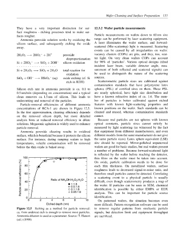
Particle-removal efficiencies of different ammonia features with known light-scattering properties and
concentrations of RCA-1 are shown in Figure 12.5. known positions on the wafer. Such standards can be
In the first approximation, cleaning efficiency depends cleaned and reused, whereas contamination standards
on the removed silicon depth, but more detailed cannot.
analysis hints at reduced removal efficiency in dilute Because real particles are not spheres with known
solutions. Megasonic agitation is widely used to enhance optical constants, particle sizes cannot strictly be
particle removal. measured by light scattering (as witnessed by the fact
Ammonia peroxide cleaning results in oxidized that equipment from different manufacturers, and even
surface, which is beneficial because it protects the silicon different models from the same manufacturer do not give
surface. For instance, during ramping wafers to high the same particle sizes). Latex sphere equivalent (LSE)
temperatures, volatile contamination will be removed size should be reported. Mirror-polished unpatterned
before the thin oxide is baked away. wafers are good for basic studies, but real wafers present
a number of problems. Because forward-scattered light
is reflected by the wafer before reaching the detector,
100 thin films on the wafer must be taken into account.
Particle removal efficiency (%) 60 Ratio of NH 4 OH:H 2 O 2 :H 2 O roughness leads to decreased signal-to-noise ratio, and
On oxide, particle calibration needs to be done for
80
each film thickness. On metallized wafers, surface
therefore small particles cannot be detected. Correlating
a scattering event to a physical particle is usually
40
difficult, even though scatterometry produces a map of
1:1:8
the wafer. If particles can be seen in SEM, chemical
0.5:1:8
20
0.05:1:8
analysis. This can be important for particle source
identification.
0 0.1:1:8 identification is possible by either EMPA or EDX
0 2 4 6 8 10 On patterned wafers, the situation becomes even
Etched depth (nm) more difficult. Pattern recognition software can be used
Figure 12.5 Etching as a method for particle removal: to remove regular patterns from stochastic particle
ca. 4 nm undercut etch is enough to remove most particles. signals, but detection limit and equipment throughput
Ammonia dilution is used as a parameter. Source: T. Hattori are sacrificed.
(ed.) (1998)