
Page 160 - Sami Franssila Introduction to Microfabrication
P. 160
Wafer Cleaning and Surface Preparation 139
0.015
d AS d SS
t AS m t SS
0.5% HF 6 h
0.010 DI rinse
Absorbance 4 h
0.005 2 h
1 h
0.25 h
0.000
3000 2950 2900 2850
−1
Wavenumber (cm )
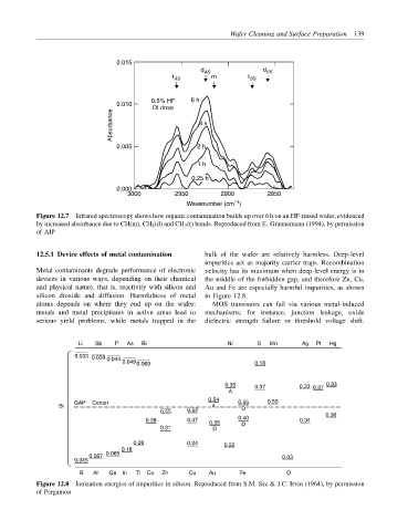
Figure 12.7 Infrared spectroscopy shows how organic contamination builds up over 6 h on an HF-rinsed wafer, evidenced
by increased absorbance due to CH(m), CH 2 (d) and CH 3 (t) bonds. Reproduced from E. Grannemann (1994), by permission
of AIP
12.5.1 Device effects of metal contamination bulk of the wafer are relatively harmless. Deep-level
impurities act as majority carrier traps. Recombination
Metal contaminants degrade performance of electronic velocity has its maximum when deep-level energy is in
devices in various ways, depending on their chemical the middle of the forbidden gap, and therefore Zn, Cu,
and physical nature, that is, reactivity with silicon and Au and Fe are especially harmful impurities, as shown
silicon dioxide and diffusion. Harmfulness of metal in Figure 12.8.
atoms depends on where they end up on the wafer: MOS transistors can fail via various metal-induced
metals and metal precipitates in active areas lead to mechanisms; for instance, junction leakage, oxide
serious yield problems, while metals trapped in the dielectric strength failure or threshold voltage shift.
Li Sb P As Bi Ni S Mn Ag Pt Hg
0.033 0.039
0.044
0.049 0.069 0.18
0.35 0.37 0.33 0.37 0.33
A
0.54
GAP Center 0.55 0.53
Si A D
0.55 0.52 0.36
0.39 0.37 0.35 0.40 0.34
0.31 D D
0.26 0.24 0.22
0.16
0.065
0.057 0.03
0.045
B Al Ga In Tl Co Zn Cu Au Fe O
Figure 12.8 Ionization energies of impurities in silicon. Reproduced from S.M. Sze & J.C. Irvin (1964), by permission
of Pergamon