
Page 155 - Sami Franssila Introduction to Microfabrication
P. 155
134 Introduction to Microfabrication
Organics can cause increased contact resistance or Measurement of native oxides can be done by
abnormal film growth. This often comes through their spectroscopic ellipsometry, but not without difficulties.
prevention of the cleaning process. When wafers are The optical constants of nanometre films are not
ramped to high-temperature processes in an oxygen- identical to thicker films and they need to be calibrated
containing atmosphere (e.g., 1% O 2 in N 2 ), organic against other methods. XPS signal strengths (Si–Si
contamination will usually be volatilized, but ramping bonds and Si–O bonds give signals at slightly different
in an inert atmosphere (N 2 or Ar) can cause carbon energies) can be used.
inclusions in the growing films or silicon carbide for- Contact angle is used to characterize surface hydro-
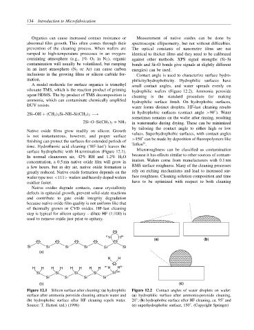
mation. philicity/hydrophobicity. Hydrophilic surfaces have
A model molecule for surface organics is trimethyl small contact angles, and water spreads evenly on
siloxane TMS, which is the reaction product of priming hydrophilic wafers (Figure 12.2). Ammonia peroxide
agent HDMS. The by-product of TMS decomposition is cleaning is the standard procedure for making
ammonia, which can contaminate chemically amplified hydrophilic surface finish. On hydrophobic surfaces,
DUV resists.
water forms distinct droplets. HF-last cleaning results
◦
in hydrophobic surfaces (contact angle >90 ). Water
2Si–OH + (CH 3 ) 3 Si–NH–Si(CH 3 ) 3 −→
sometimes remains on the wafer after rinsing, resulting
2Si–O–Si(CH 3 ) 3 + NH 3 in watermarks during drying. These can be minimized
by tailoring the contact angle to either high or low
Native oxide films grow readily on silicon. Growth
is not instantaneous, however, and proper surface values. Superhydrophobic surfaces, with contact angles
◦
finishing can protect the surfaces for extended periods of >150 can be made by deposition of fluoropolymers like
time. Hydrofluoric acid cleaning (‘HF-last’) leaves the Teflon .
surface hydrophobic with H-termination (Figure 12.1). Microroughness can be classified as contamination
In normal cleanroom air, 42% RH and 1.2% H 2 O because it has effects similar to other sources of contam-
concentration, a 0.5 nm native oxide film will grow in ination. Wafers come from manufacturers with 0.1 nm
RMS surface roughness. Many of the cleaning processes
a few hours, but in dry air, native oxide formation is
greatly reduced. Native oxide formation depends on the rely on etching mechanisms and lead to increased sur-
wafer type too: <111> wafers and heavily doped wafers face roughness. Cleaning solution composition and time
oxidize faster. have to be optimized with respect to both cleaning
Native oxides degrade contacts, cause crystallinity
defects in epitaxial growth, prevent solid-state reactions
and contribute to gate oxide integrity degradation
because native oxide film quality is not uniform like that
of thermally grown or CVD oxides. HF-last cleaning
step is typical for silicon epitaxy – dilute HF (1:100) is
used to remove oxide just prior to epitaxy.
• •
• O •
δ+ H H δ+
• • • • • • • • • • (a) (b)
• O • • O • • O • • O • • O •
Si Si Si Si Si Si
(a)
H H
• O• •
•
H H H H H H H H e− H H e−
Si Si Si Si Si 2e+
Si Si Si Si
(b) (c)
Figure 12.1 Silicon surface after cleaning: (a) hydrophilic Figure 12.2 Contact angles of water droplets on wafer:
surface after ammonia peroxide cleaning attracts water and (a) hydrophilic surface after ammonia-peroxide cleaning,
◦
◦
(b) hydrophobic surface after HF cleaning repels water. 20 ; (b) hydrophobic surface after HF cleaning, ca. 95 and
Source: T. Hattori (ed.) (1998) (c) superhydrophobic surface, 150 . (Copyright Springer)
◦