Page 152 - Sami Franssila Introduction to Microfabrication
P. 152
Etching 131


           4. How much underlying oxide is lost when a tungsten
                                                                Profile       A:S selectivity
             film of 500 nm thickness is etched from a sample that
             has 300 nm steps on it? Tungsten: oxide selectivity  anisotropic    ∞
             is 10:1.                                           anisotropic      5:1
           5. Etch rate could basically be measured easily by   anisotropic      1:1
                                                                isotropic        ∞
             weighing the sample before and after etching, and
                                                                isotropic        5:1
             translating that into the rate by taking the area into
                                                                isotropic        1:1
             account. What resolution scale is needed to determine
             rates for:
                                                       9. How much dimensional error does chromium wet
              – tungsten etching, 500 nm thickness       etching introduce to (a) 1X photomasks and (b) 5X
              – silicon etching, 20 nm thickness.        reticles?
                                3
             Densities: W – 19.5 g/cm , Si – 2.65 g/cm 3
           6. How can the porosity of porous silicon be measured  REFERENCES AND RELATED READINGS
             by weighing?
                                                       Bell, F.H. & O. Joubert: Polysilicon gate etching in high
           7. What is the resistivity of the p-type wafer shown in  density plasmas, J. Vac. Sci. Technol., B14 (1996), 3473.
             Figure 11.6(b)?
                                                       Bien, D.C.S. et al: Characterization of masking materials for
           8. Draw cross-sectional figures of the shown structure  deep glass etching, J. Micromech. Microeng., 13 (2003), S34.
             under the following etch conditions, for two etch  Collins, S.D.: Etch stop techniques for micromachining, J.
             times: right at etch end point; and after 50%  Electrochem. Soc., 144 (1997), 2242.
             overetch.                                 Hsiao, R.: Fabrication of magnetic recording heads and dry
                                                        etching of head materials, IBM J. Res. Dev., 43 (1999), 89.
                                                       Kim, B.-H. et al: MEMS fabrication of high aspect ratio track-
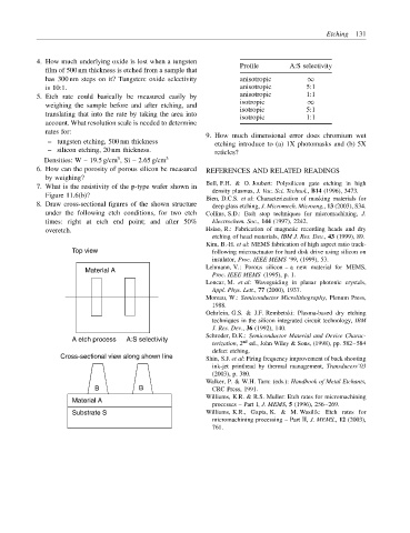
                    Top view                            following microactuator for hard disk drive using silicon on
                                                        insulator, Proc. IEEE MEMS ‘99, (1999), 53.
                       Material A                      Lehmann, V.: Porous silicon – a new material for MEMS,
                                                        Proc. IEEE MEMS (1995), p. 1.
                                                       Loncar, M. et al: Waveguiding in planar photonic crystals,
                                                        Appl. Phys. Lett., 77 (2000), 1937.
                                                       Moreau, W.: Semiconductor Microlithography, Plenum Press,
                                                        1988.
                                                       Oehrlein, G.S. & J.F. Rembetski: Plasma-based dry etching
                                                        techniques in the silicon integrated circuit technology, IBM
                                                        J. Res. Dev., 36 (1992), 140.
                    A etch process   A:S selectivity   Schroder, D.K.: Semiconductor Material and Device Charac-
                                                        terization, 2 nd  ed., John Wiley & Sons, (1998), pp. 582–584
                                                        defect etching.
                 Cross-sectional view along shown line  Shin, S.J. et al: Firing frequency improvement of back shooting
                                                        ink-jet printhead by thermal management, Transducers’03
                                                        (2003), p. 380.
                                                       Walker, P. & W.H. Tarn: (eds.): Handbook of Metal Etchants,
                          B          B                  CRC Press, 1991.
                    Material A                         Williams, K.R. & R.S. Muller: Etch rates for micromachining
                                                        processes – Part I, J. MEMS, 5 (1996), 256–269.
                    Substrate S                        Williams, K.R., Gupta, K. & M. Wasilik: Etch rates for
                                                        micromachining processing – Part II, J. MEMS., 12 (2003),
                                                        761.

