
Page 149 - Sami Franssila Introduction to Microfabrication
P. 149
128 Introduction to Microfabrication
In plasma etch simulation, plasma physics provides 11.5.2 Selectivity
ion and neutral energies, diffusion models are needed
for fluxes of particles impinging on the surface, and Selectivity is a measure of etch rate ratios (ERR).
then the surface reactions need to be understood. Selectivity can be defined between film and substrate
and between film and photoresist or other masking
There can be competing reactions at every stage: SF 6
molecules are ionized in plasma, but F − ions can materials. Selectivities range from 1:1 to 100:1 in typical
react with oxygen in the plasma, which decreases plasma etching processes. Resist selectivities range from
active fluorine concentration; CHF 3 acts not only as 1:1 to 10:1 in plasma etching (with 100:1 possible). In
wet etching, resist selectivity is often good, but resist
a fluorine source, but also as a source of (CF 2 ) n
polymer, which will deposit on the wafer. Simple adhesion loss and peel-off are severe limitations.
model systems such as argon bombardment of fluori- Etch stop is the term used for etching processes, in
nated silicon surfaces have been simulated but predic- which the selectivity is so high that etching essentially
tive first principles plasma etch simulators remain to stops when the underlying material is reached. This will
be developed. be discussed more in the Chapter 21, because it has
important applications in bulk micromechanics. When
polymeric films are etched, selectivity and photoresist
stripping are problematic: resist is polymeric material
11.5 CHARACTERIZATION OF ETCH PROCESSES
too and selectivity between two similar materials is
11.5.1 Linewidth and profile difficult to achieve. PECVD oxide or nitride layers, can
be used to cap polymer layers.
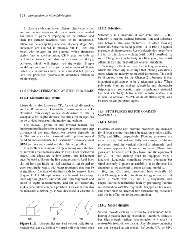
Linewidth is also known as CD, for critical dimension,
in the IC industry. Linewidth measurement checks
deviation from design values. A deviation of 10% is 11.6 ETCH PROCESSES FOR COMMON
acceptable for digital devices, but this error budget has MATERIALS
to be divided between lithography and etching. 11.6.1 Silicon
The sidewall profile of the finished feature has
important implications for subsequent process steps: step Fluorine, chlorine and bromine processes are standard
coverage of the next deposition process depends on for silicon etching, resulting in reaction products SiF 4 ,
it. The profile can be measured with top view optical SiCl 4 and SiBr 4 , respectively. Fluorine processes are
or SEM measurements, but destructive cross-sectional safer to use, but seldom fully anisotropic. Chlorine
SEM pictures are considered the ultimate profiles. processes result in vertical sidewalls inherently, and
Linewidth can be measured by scanning over the line the same applies to bromine processes. These two
either with a mechanical stylus or with a laser or electron gases are, however, are highly toxic, and the equipment
beam. Line edges are seldom abrupt, and judgement for Cl 2 or HBr etching must be equipped with a
must be used to locate the line edge properly. Real lines loadlock. Loadlocks complicate system operation but
do not have perfectly vertical sidewalls, but sloped or simultaneously improve repeatability since the reaction
even retrograde walls, with edge roughness that can be chamber is not exposed to room air and humidity.
a significant fraction of the linewidth for narrow lines SF 6 - and CF 4 -based processes have typically 10
(Figure 11.11). Multiple scans must be made to average to 40% oxygen added to them. Oxygen has several
over edge roughness. Substrate and film roughness add roles: it reacts with SF n and CF n fragments, and
noise to stylus measurements, and for soft materials, keeps fluorine concentration high by preventing fluorine
stylus penetration can be a problem. Linewidth can also recombination with the fragments. Oxygen etches resist,
be measured electrically, as was discussed in Chapter 2. and contributes to sidewall film formation by oxidation
and via its effect on resist consumption.
11.6.2 Silicon dioxide
Silicon dioxide etching is driven by ion bombardment.
Isotropic plasma etching of oxide is, therefore, difficult,
(a) (b) (c) but high-enough radical concentration will result in
Figure 11.11 Line profiles (a) ideal vertical wall; (b) ret- reasonable isotropic etch rates. Any fluorine-containing
rograde wall and (c) positively sloped wall with rough edge gas can be used as an etchant for oxide, CF 4 or SF 6 ,