
Page 146 - Sami Franssila Introduction to Microfabrication
P. 146
Etching 125
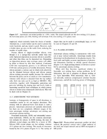
(111)
(111)
54.7° (100)
Figure 11.7 Anisotropic wet-etched profiles in <100> wafer. The sloped sidewalls are the slow-etching (111) planes;
the horizontal planes are (100). Etching will terminate if the slow-etching (111) planes meet
employed, which seriously limits the choice of metals. shapes that can be made is astonishingly large, as will
Alternatively, a wafer holder can be used to protect the be seen in Chapters 21 and 28.
wafer backside, and any metal is good. However, such
a holder takes up area on the wafer front, reducing the
number of usable chips. 11.4 PLASMA ETCHING
Porous silicon is single-crystalline silicon, even
though it is a sponge-like network rather than true Anisotropic plasma etching is synonymous with verti-
solid. Epitaxial deposition on porous silicon is possible, cal or near vertical sidewalls. Anisotropy results from
and other thin films can be deposited too. Depending directional ion bombardment in the plasma reactor. Ver-
on deposition process step coverage, pores will either tical walls and highly accurate reproduction of photore-
be filled or buried by thin film material. Conformal sist dimensions translate to closely spaced structures
CVD into macroporous grooves is no different from (Figure 11.8). High packing density of devices is possi-
CVD into etched grooves of similar dimensions. Porous ble by anisotropic plasma etching.
silicon presents a curious case in which etch selectivity When etch bias becomes significant relative to
linewidth, wet etching faces serious problems. In IC
can be obtained between silicon and silicon: porous
fabrication, this led to adoption of plasma etching at
silicon etching proceeds rapidly because the sidewalls
ca. 3 µm linewidths. With anisotropy, that is, verti-
between the pores can be as small as a few nanometres,
cal sidewalls, undercut compensation schemes became
whereas solid silicon is attacked from the top surface
only. Etch rate ratio can be as high as 100 000:1. This unnecessary, and all the resolving power of lithography
selectivity, together with lithographic patterning and
pore-size tailoring (by doping type and level), leads to
interesting sacrificial layer techniques in which porous
silicon is etched away underneath solid silicon. This will
be dealt with in Chapter 22.
11.3 ANISOTROPIC WET ETCHING
(a) (b)
Isotropy, or homogeneity of space in all directions, is
sometimes useful as we can neglect directions. Wet
etching with its spherical-wave etch fronts is such a
process. Anisotropic processes are spatially directional,
but there are two completely different usages of the
term anisotropic etching: anisotropic wet etching and
anisotropic plasma etching.
Potassium hydroxide, KOH, and tetramethyl ammo-
nium hydroxide, TMAH, are the common anisotropic
wet etchants for silicon. In KOH etching, the rates of (c)
different crystal planes can differ by a factor of 200. Figure 11.8 Plasma-etched anisotropic profiles (a) ideal
Silicon (100) crystal planes are fast etching, whereas vertical; (b) practical vertical with a slight undercut of
(111) planes are slow etching. This results in structures the mask and sloped sidewall and (c) SEM micrograph of
bound by the (111) planes (Figure 11.7). The variety of RIE profile