
Page 144 - Sami Franssila Introduction to Microfabrication
P. 144
Etching 123
4. Etching reaction is exothermic and temperature rises suitable masking materials for concentrated HF (49%).
during etching (for these reactions, stirring decreases Silicon carbide (PECVD SiC), tantalum pentoxide
the etch rate because it decreases temperature). (Ta 2 O 5 ) and aluminium nitride (AlN) are excellent
5. Evaporation leads to concentration changes dur- hard masks for many wet and dry etching processes.
ing etching. Aluminum nitride, however, is easily etched by alkaline
solutions such as KOH or even dilute NaOH photoresist
developer. This fact can sometimes make processing
11.1.3 Etching with a hard mask much faster and easier compared to other hard masks,
which are very stable materials (which is why they were
In wet etching the resist is usually not consumed by the chosen in the first place).
etchant, and the gravest danger is adhesion loss. This is
dependent on priming, feature size, resist thickness and
the chemical character of the resist. Generally, thicker
resists are mechanically more stable. Interface stability 11.2 ELECTROCHEMICAL ETCHING
is important for the etched profile because the etchant
can easily propagate along the film/resist interface. Silicon is not etched in HF. If, however, silicon is
Photoresists are materials that combine photoac- made an anode in an electrochemical etching set-up,
tivity and mechanical/thermal/chemical stability, and, etch rates of ca. 1 µm/min are observed. Depending
obviously, photoactivity is the property that cannot on current density, silicon can be etched in two rather
different modes: pore formation and electropolishing. In
be sacrificed. In order to find optimum materials as
pore formation, etching proceeds vertically downwards,
etch/plating/implant masks, the concept of hard mask
leaving a silicon ‘skeleton’ with up to 80% empty space.
has been devised. The mask material is etched with
Electropolishing resembles wet etching, in the sense that
photoresist masking, the photoresist is then stripped
and the etch/plating/implant process is performed using the whole surface is being etched.
the hard mask only. The hard mask material can be The electrochemical etch set-up is shown in
optimized to suit the application, irrespective of the Figure 11.5. Hydrofluoric acid, with or without ethanol
photoresist. and/or water is used as an electrolyte. Platinum is
The wet etchant for Si 3 N 4 is boiling concentrated the standard cathode. Both electropolishing and pore
◦
phosphoric acid (H 3 PO 4 ) at 180 C. The photoresist formation take place in the anodic regime.
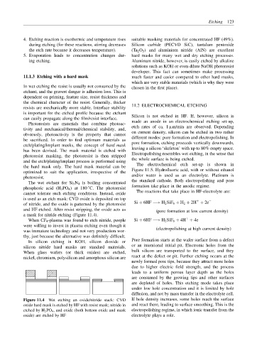
cannot tolerate such etching conditions. Instead, oxide The reactions that take place in HF-electrolyte are:
is used as an etch mask: CVD oxide is deposited on top + −
of nitride, and the oxide is patterned by the photoresist Si + 6HF −→ H 2 SiF 6 + H 2 + 2H + 2e
and HF-etched. After resist stripping, the oxide acts as (pore formation at low current density)
a mask for nitride etching (Figure 11.4).
+
When CF 4 -plasma was found to etch nitride, people Si + 6HF −→ H 2 SiF 6 + 4H + 4e −
were willing to invest in plasma etching even though it
was immature technology and not very production wor- (electropolishing at high current density)
thy, just because the alternative was definitely difficult.
Pore formation starts at the wafer surface from a defect
In silicon etching in KOH, silicon dioxide or
or an intentional initial pit. Electronic holes from the
silicon nitride hard masks are standard materials.
When glass wafers (or thick oxides) are etched, bulk silicon are transported to the surface, and they
nickel, chromium, polysilicon and amorphous silicon are react at the defect or pit. Further etching occurs at the
newly formed pore tips, because they attract more holes
due to higher electric field strength, and the process
leads to a uniform porous layer depth as the holes
are consumed by the growing tips and other surfaces
are depleted of holes. This etching mode takes place
under low hole concentration and it is limited by hole
diffusion, and not by mass transfer in the electrolyte cell.
Figure 11.4 Wet etching an oxide/nitride stack: CVD If hole density increases, some holes reach the surface
oxide hard mask is etched by HF with resist mask; nitride in and react there, leading to surface smoothing. This is the
etched by H 3 PO 4 , and oxide (both bottom oxide and mask electropolishing regime, in which ionic transfer from the
oxide) are etched by HF electrolyte plays a role.