
Page 145 - Sami Franssila Introduction to Microfabrication
P. 145
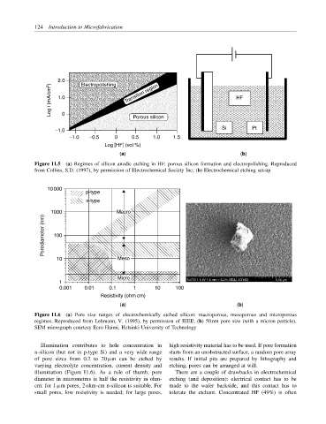
124 Introduction to Microfabrication


                    2.0     Electropolishing
                  Log i (mA/cm 2 )  1.0   Transition region                    HF


                     0
                                             Porous silicon
                                                                          Si Si     Pt Pt
                   −1.0
                        −1.0  −0.5     0    0.5    1.0    1.5
                                   Log [HF] (vol %)
                                        (a)                                     (b)
            Figure 11.5 (a) Regimes of silicon anodic etching in HF: porous silicon formation and electropolishing. Reproduced
            from Collins, S.D. (1997), by permission of Electrochemical Society Inc; (b) Electrochemical etching set-up


                 10000
                             p-type
                             n-type
                  1000                 Macro
               Porediameter (nm)  100


                    10                  Meso


                                        Micro                 S4700 1.5 kV 7.6 mm × 8.21k SE(L) 3/31/03
                     1                                                                      5.00 µm
                     0.001   0.01    0.1     1      10     100
                                  Resistivity (ohm cm)
                                        (a)                                    (b)
            Figure 11.6 (a) Pore size ranges of electrochemically etched silicon: macroporous, mesoporous and microporous
            regimes. Reproduced from Lehmann, V. (1995), by permission of IEEE; (b) 50 nm pore size (with a micron particle).
            SEM micrograph courtesy Eero Haimi, Helsinki University of Technology

              Illumination contributes to hole concentration in  high resistivity material has to be used. If pore formation
            n-silicon (but not in p-type Si) and a very wide range  starts from an unobstructed surface, a random pore array
            of pore sizes from 0.2 to 20 µm can be etched by  results. If initial pits are prepared by lithography and
            varying electrolyte concentration, current density and  etching, pores can be arranged at will.
            illumination (Figure 11.6). As a rule of thumb, pore  There are a couple of drawbacks in electrochemical
            diameter in micrometres is half the resistivity in ohm-  etching (and deposition): electrical contact has to be
            cm: for 1 µm pores, 2 ohm-cm n-silicon is suitable. For  made to the wafer backside, and this contact has to
            small pores, low resistivity is needed; for large pores,  tolerate the etchant. Concentrated HF (49%) is often