
Page 251 - Sami Franssila Introduction to Microfabrication
P. 251
230 Introduction to Microfabrication
Stability of sidewall pillars is determined by stresses
in the film and pillar length-height-width ratio. Aspect
ratios of 5:1 can be made fairly easily. Small holes and
apertures can be made by sidewall spacer removal, as
shown for nanofilter of Figure 22.1.
23.4 LOCALIZED DEPOSITION
Most thin film deposition methods are blanket deposi-
Figure 23.9 Deposition with a shadow mask
tions, that is, film deposits everywhere on the wafer. A
handful of techniques provide selective area deposition.
Chemical differences in microstructures form the basis
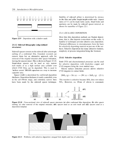
23.3.2 Sidewall lithography (edge-defined
for selectively depositing material on just one of the sur-
structures)
faces. Selective deposition has many attractive features,
Sidewall spacers remain on the sidewall after anisotropic simplicity of process integration being the foremost.
etching of a conformal film. Extended overetch can
remove them but an alternative approach calls for
removal of the original structure after spacer formation, 23.4.1 Selective deposition
leaving the spacers intact. This is shown in Figure 23.10. Both CVD and electrochemical processes can be used
Stand-alone spacers can be used as very narrow for selective deposition, with electroless copper and
etch masks or as a high surface area cylinder over CVD tungsten being the most studied ones.
which CVD films can be deposited. This is used in Silicon surface reduction process allows selective
‘hollow crown’ DRAM capacitors as a way to increase CVD tungsten in contact holes
capacitor area.
Spacer width is determined by conformal deposition 2WF 6 (g) + 3Si (s) −→ 2W (s) + 3SiF 4 (g) (23.1)
thickness. Deposition thickness is easily controlled, even
in the sub-100 nm range, and extremely narrow lines This reaction is selective because SiO 2 does not reduce
have been made by the sidewall spacer technique. WF 6 . However, ca. 20 nm of silicon is consumed,
(d1)
(d2)
(a) (b) (c)
Figure 23.10 Cross-sectional view of sidewall spacer structures (a) after conformal film deposition; (b) after spacer
etching; (c) after removal of the original structure; (d1) spacers used as an etch mask and (d2) spacers used as a
deposition template
Figure 23.11 Problems with selective deposition: unequal hole depths and loss of selectivity