
Page 248 - Sami Franssila Introduction to Microfabrication
P. 248
23
Structures by Deposition
The standard approach in microfabrication is to deposit
film all over the wafer and then remove unwanted
parts by etching or polishing. In this chapter, various
techniques for direct and localized structure formation
by deposition are presented. They are for the most part,
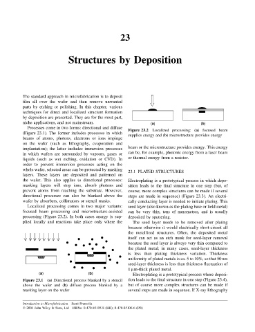
niche applications, and not mainstream. (a) (b)
Processes come in two forms: directional and diffuse Figure 23.2 Localized processing: (a) focused beam
(Figure 23.1). The former includes processes in which supplies energy and (b) microstructure provides energy
beams of atoms, photons, electrons or ions impinge
on the wafer (such as lithography, evaporation and
implantation); the latter includes immersion processes beam or the microstructure provides energy. This energy
in which wafers are surrounded by vapours, gases or can be, for example, photonic energy from a laser beam
liquids (such as wet etching, oxidation or CVD). In or thermal energy from a resistor.
order to prevent immersion processes acting on the
whole wafer, selected areas can be protected by masking 23.1 PLATED STRUCTURES
layers. These layers are deposited and patterned on
the wafer. This also applies to directional processes: Electroplating is a prototypical process in which depo-
masking layers will stop ions, absorb photons and sition leads to the final structure in one step (but, of
prevent atoms from reaching the substrate. However, course, more complex structures can be made if several
directional processes can also be blanked above the steps are made in sequence) (Figure 23.3). An electri-
wafer by absorbers, collimators or stencil masks. cally conducting layer is needed to initiate plating. This
Localized processing comes in two major variants: seed layer (also known as the plating base or field metal)
focused beam processing and microstructure-assisted can be very thin, tens of nanometres, and is usually
processing (Figure 23.2). In both cases energy is sup- deposited by sputtering.
plied locally and reactions take place only where the The seed layer needs to be removed after plating
because otherwise it would electrically short-circuit all
the metallized structures. Often, the deposited metal
itself can act as an etch mask for seed-layer removal
because the seed layer is always very thin compared to
the plated metal; in many cases, seed-layer thickness
is less than plating thickness variation. Thickness
uniformity of plated metals is ca. 5 to 10%, so that 50 nm
seed-layer thickness is less than thickness fluctuation of
1 µm-thick plated metal.
(a) (b) Electroplating is a prototypical process where deposi-
Figure 23.1 (a) Directional process blanked by a stencil tion leads to the final structure in one step (Figure 23.4),
above the wafer and (b) diffuse process blanked by a but of course more complex structures can be made if
masking layer on the wafer several steps are made in sequence. If X-ray lithography
Introduction to Microfabrication Sami Franssila
2004 John Wiley & Sons, Ltd ISBNs: 0-470-85105-8 (HB); 0-470-85106-6 (PB)