
Page 244 - Sami Franssila Introduction to Microfabrication
P. 244
Sacrificial and Released Structures 223
Poly Si Polyimide
Polyimide
Aluminum Polysilicon
PSG
Si wafer Glass substrate
(a) (b)
Figure 22.12 (a) A polyimide hinge joins static and moving polysilicon plates and (b) polyimide hinged, electrostatically
actuated mirror. Reproduced from Suzuki, K. et al. (1994), by permission of IEEE
The material of the structural layer can be, for
instance silicon nitride, but epitaxial silicon can also be
used. Porous silicon is single-crystalline silicon and it is
possible to grow epitaxial film on it.
Porous silicon is a mechanically weak material, and
it can be destroyed by the capillary forces during drying
(a) (b) (cf. stiction where capillary forces pull free-standing
structures together upon drying). Porous silicon can be
Figure 22.13 Two-poly staple hinge: (a) side view and
(b) top view. Adapted from Pister, K. et al. (1992), by destroyed by gas bubbles as well: KOH etching releases
permission of Elsevier hydrogen (Equation 11.1), and if gas evolution is rapid,
the bubbles can burst porous structures. For this reason
dilute KOH, 0.1 to 1%, is used rather than 20 to 50%,
22.7 SACRIFICIAL STRUCTURES USING which is typical of silicon anisotropic etching.
POROUS SILICON In a modification of the above scheme, a free-standing
structure can be made of bulk single-crystal silicon. The
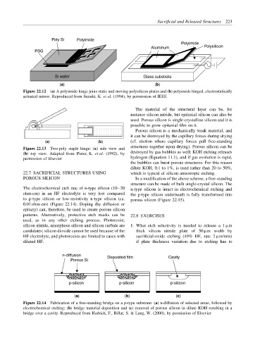
The electrochemical etch rate of n-type silicon (10–20 n-type silicon is intact in electrochemical etching and
ohm-cm) in an HF electrolyte is very low compared the p-type silicon underneath is fully transformed into
to p-type silicon or low-resistivity n-type silicon (ca. porous silicon (Figure 22.15).
0.01 ohm-cm) (Figure 22.14). Doping (by diffusion or
epitaxy) can, therefore, be used to create porous silicon
patterns. Alternatively, protective etch masks can be 22.8 EXERCISES
used, as in any other etching process. Photoresist,
silicon nitride, amorphous silicon and silicon carbide are 1. What etch selectivity is needed to release a 1 µm
candidates; silicon dioxide cannot be used because of the thick silicon nitride plate of 50 µm width by
HF electrolyte, and photoresists are limited to cases with sacrificial-oxide etching (49% HF, rate 2 µm/min)
diluted HF. if plate thickness variation due to etching has to
n-diffusion Deposited film Cavity
Porous Si
p-silicon p-silicon p-silicon
(a) (b) (c)
Figure 22.14 Fabrication of a free-standing bridge on a p-type substrate: (a) n-diffusion of selected areas, followed by
electrochemical etching; (b) bridge material deposition and (c) removal of porous silicon in dilute KOH resulting in a
bridge over a cavity. Reproduced from Hedrich, F., Billat, S. & Lang, W. (2000), by permission of Elsevier