
Page 242 - Sami Franssila Introduction to Microfabrication
P. 242
Sacrificial and Released Structures 221
large. Alternatively, capacitance change between the
finger plates can be used for sensing, for example, in
accelerometers and gyroscopes. (a)
It is possible to make such a comb drive in a one
mask, single structural-layer process if the fixed comb
(g)
dimensions were designed to be much larger than those
of the movable comb; in fact, the whole fixed comb
(b)
should be considered as an anchor. However, such
a process has too many design limitations for it to
be useful. A two-layer, four-mask process described
in Figure 22.8 and outlined below offers a robust
(c)
fabrication process for comb drives.
(h)
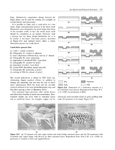
Comb-drive process flow
(a) oxide + nitride insulation
(b) lithography #1: contact to substrate (d)
+
(c) poly1 deposition (300 nm thick, heavily n doped)
(d) lithography #2: poly1 patterning
(e) deposition of sacrificial PSG, 2 µm thick (i)
(f) lithography #3: anchors for poly2
(g) deposition of poly2, 2 µm thick (e)
(h) second PSG deposition, anneal and etch
(i) lithography #4: patterning of poly2
(j) etching of PSG for release of poly2.
The second polysilicon is doped by PSG from top, (f) (j)
eliminating dopant gradient effects. In addition to
doping, the annealing step also has the role of poly2 SiO 2 Polysilicon
stress optimization. Both the fixed and the movable Si 3 N 4 PSG
comb are defined in the same photolithography step, and Figure 22.8 Fabrication of a comb-drive structure in a
thus their spacing is free of alignment errors. two structural–layer process. Reproduced from Tang, W.C.
Two structural–layer processes offer similar device et al. (1989), by permission of IEEE
and fabrication benefits in metal micromechanics. Elec-
troplated metals can serve both as structural layers selectively removed under nickel or gold, enabling elab-
and as sacrificial layers, for example, copper can be orate 3D structures to be made, Figure 22.9.
(a) (b)
Figure 22.9 (a) 3D inductor coil with copper bottom and nickel bridge structural layers and (b) 3D transformer with
Cu-bottom and copper bridge with Ni-core by three structural layers. Reproduced from Yoon, J.-B. et al. (1998), by
permission of Institute of Pure and Applied Physics