
Page 238 - Sami Franssila Introduction to Microfabrication
P. 238
22
Sacrificial and Released Structures
In many cases, films and structures are used inter-
mittently, only to be disposed of in the next process
+
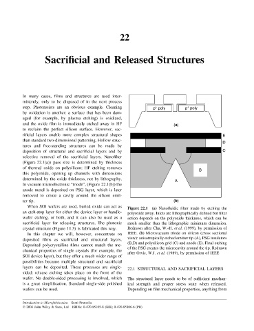
step. Photoresists are an obvious example. Cleaning p poly p poly
+
by oxidation is another: a surface that has been dam-
aged (for example, by plasma etching) is oxidized,
and the oxide film is immediately etched away in HF (a)
to reclaim the perfect silicon surface. However, sac-
rificial layers enable more complex structural shapes E
than standard two-dimensional patterning. Hollow struc- D
tures and free-standing structures can be made by
deposition of structural and sacrificial layers and by C
selective removal of the sacrificial layers. Nanofilter
(Figure 22.1(a)) pass size is determined by thickness
of thermal oxide on polysilicon: HF etching removes B
this polyoxide, opening up channels with dimensions
determined by the oxide thickness, not by lithography. A
In vacuum microelectronic “triode”, (Figure 22.1(b)) the
anode metal is deposited on PSG layer, which is later
removed to create a cavity around the silicon emit-
ter tip. (b)
When SOI wafers are used, buried oxide can act as
Figure 22.1 (a) Nanofluidic filter made by etching the
an etch-stop layer for either the device layer or handle- polyoxide away. Inlets are lithographically defined but filter
wafer etching, or both, and it can also be used as a action depends on the polyoxide thickness, which can be
sacrificial layer for releasing structures. The photonic much smaller than the lithographic minimum dimension.
crystal structure (Figure 11.3) is fabricated this way. Redrawn after Chu, W.-H. et al. (1999), by permission of
In this chapter we will, however, concentrate on IEEE. (b) Microvacuum triode on silicon (cross sectional
deposited films as sacrificial and structural layers. view): anisotropically etched emitter tip (A), PSG insulators
(B,D) and polysilicon grid (C) and anode (E). Final etching
Deposited polycrystalline films cannot match the me-
of the PSG creates the microcavity around the tip. Redrawn
chanical properties of single crystals (for example, the
after Orvis, W.J. et al. (1989), by permission of IEEE
SOI device layer), but they offer a much wider range of
possibilities because multiple structural and sacrificial
layers can be deposited. These processes are single- 22.1 STRUCTURAL AND SACRIFICIAL LAYERS
sided: release etching takes place on the front of the
wafer. No double-sided processing is involved, which The structural layer needs to be of sufficient mechan-
is a great simplification. Standard single-side polished ical strength and proper stress state when released.
wafers can be used. Depending on film mechanical properties, anything from
Introduction to Microfabrication Sami Franssila
2004 John Wiley & Sons, Ltd ISBNs: 0-470-85105-8 (HB); 0-470-85106-6 (PB)