
Page 236 - Sami Franssila Introduction to Microfabrication
P. 236
Wet-etched Silicon Structures 215
[111]
<100> <110> <111>
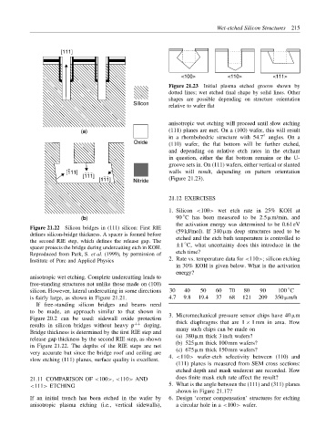
Figure 21.23 Initial plasma etched groove shown by
dotted lines; wet etched final shape by solid lines. Other
shapes are possible depending on structure orientation
Silicon
relative to wafer flat
anisotropic wet etching will proceed until slow etching
(a) (111) planes are met. On a (100) wafer, this will result
◦
in a rhombohedric structure with 54.7 angles. On a
Oxide (110) wafer, the flat bottom will be further etched,
and depending on relative etch rates in the etchant
in question, either the flat bottom remains or the U-
groove sets in. On (111) wafers, either vertical or slanted
[111] walls will result, depending on pattern orientation
[111]
[111] Nitride (Figure 21.23).
21.12 EXERCISES
1. Silicon <100> wet etch rate in 25% KOH at
◦
(b) 90 C has been measured to be 2.5 µm/min, and
the activation energy was determined to be 0.61 eV
Figure 21.22 Silicon bridges in (111) silicon: First RIE
defines silicon-bridge thickness. A spacer is formed before (59 kJ/mol). If 340 µm deep structures need to be
the second RIE step, which defines the release gap. The etched and the etch bath temperature is controlled to
◦
spacer protects the bridge during undercutting etch in KOH. ±1 C, what uncertainty does this introduce in the
Reproduced from Park, S. et al. (1999), by permission of etch time?
Institute of Pure and Applied Physics 2. Rate vs. temperature data for <110>; silicon etching
in 30% KOH is given below. What is the activation
energy?
anisotropic wet etching. Complete undercutting leads to
free-standing structures not unlike those made on (100)
◦
silicon. However, lateral undercutting in some directions 30 40 50 60 70 80 90 100 C
is fairly large, as shown in Figure 21.21. 4.7 9.8 19.4 37 68 121 209 350 µm/h
If free-standing silicon bridges and beams need
to be made, an approach similar to that shown in
Figure 20.2 can be used: sidewall oxide protection 3. Micromechanical pressure sensor chips have 40 µm
results in silicon bridges without heavy p ++ doping. thick diaphragms that are 1 × 1 mm in area. How
Bridge thickness is determined by the first RIE step and many such chips can be made on
release gap thickness by the second RIE step, as shown (a) 380 µm thick 3 inch wafers?
in Figure 21.22. The depths of the RIE steps are not (b) 525 µm thick 100 mm wafers?
very accurate but since the bridge roof and ceiling are (c) 675 µm thick 150 mm wafers?
slow etching (111) planes, surface quality is excellent. 4. <110> wafer-etch selectivity between (110) and
(111) planes is measured from SEM cross sections:
etched depth and mask undercut are recorded. How
21.11 COMPARISON OF <100>, <110> AND does finite mask etch rate affect the result?
<111> ETCHING 5. What is the angle between the (111) and (311) planes
shown in Figure 21.17?
If an initial trench has been etched in the wafer by 6. Design ‘corner compensation’ structures for etching
anisotropic plasma etching (i.e., vertical sidewalls), a circular hole in a <100> wafer.