
Page 235 - Sami Franssila Introduction to Microfabrication
P. 235
214 Introduction to Microfabrication
Si (111) Oxidization
[111] [111]
[111] (110)
(011) (101) Patterning
A′ 19.47°
A A
(101) (011)
[111] (110)
[111] [111] Dry etching
Flat
A′ A′ [110] <110>
(111)
120° 60° Cross section A A′
Etching
A
by EPW
60°
[111]
Baking of
solution
Top view Side view
(a)
Stripping of
laser cavity
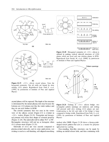
Figure 21.20 Hexagonal symmetry of <111> silicon is
[101] utilized in making vertical sidewall structures of (110)
planes which are local etch rate minima planes in EPW.
[110] B 60° Reproduced from Sasaki, M. et al. (2000), by permission
B′
[011] of Institute of Pure and Applied Physics
[111]
B′ 120° B
90° 90°
60° Flat
(111)
[110] Pattern openings
Cross section A A′
[101] B′
B [110]
[111]
[011]
C′
[111]
Top view Side view [111]
(b)
Figure 21.19 <111> silicon crystal planes. Note the
hexagonal symmetry. Not all walls are bound by slow C
etching (111) planes. Reproduced from Park, S. et al. Flat
[110]
(1999), by permission of Institute of Pure and Applied
Physics [111]
[111]
[111]
crystal planes will be exposed. The depth of the structure
is determined by the initial plasma etch step because the Figure 21.21 Etching of <111> silicon bridge: two
bottoms are (111) planes just like the wafer surface and
rectangular pattern openings are undercut, and etching
they do not etch further in KOH. will proceed until slow etching (111) planes are met.
The sixfold symmetry that was seen in the vertex Undercutting to the left and right of the bridge is large
view of the silicon crystal (Figure 4.5) is evident in compared to bridge width. Reproduced from Park, S. et al.
<111> wafers (Figure 21.19). Triangular and hexago- (1999), by permission of Institute of Pure and Applied
nal patterns will retain their shapes if oriented properly Physics
◦
◦
(Figure 21.20). The sidewalls will be either 70.5 or 90 .
Rectangular structures will end up as hexagons when method after DRIE. Figure 21.20 shows a honeycomb-
(111) planes meet (Figure 21.21). shaped trench pattern that acts as a master for polymer
Sidewalls of (111) are very smooth compared to optical-device casting.
plasma-etched sidewalls, and in some applications, wet Free-standing thin-film structures can be made by
etching is used as a self-limiting, self-aligned smoothing etching an initial release hole, and then continuing with