
Page 230 - Sami Franssila Introduction to Microfabrication
P. 230
Wet-etched Silicon Structures 209
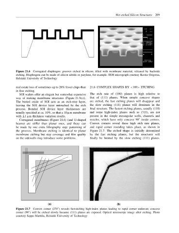
Figure 21.6 Corrugated diaphragm: grooves etched in silicon, filled with membrane material, released by backside
etching. Diaphragms can be made of silicon nitride or parylene, for example. SEM micrograph courtesy Kestas Grigoras,
Helsinki University of Technology
real estate loss of sometimes up to 20% fewer chips than 21.6 COMPLEX SHAPES BY <100> ETCHING
in free etching.
SOI wafers offer an elegant but somewhat expensive The etch rate of (100) planes is high relative to
way of making membrane structures (Figure 21.5(c)). that of (111) planes. When simple concave shapes
The buried oxide of SOI acts as an etch-stop layer, are etched, the fast etching planes will disappear and
leaving the SOI device layer untouched by the etch the slow etching (111) planes will dominate in the
process. Bonded SOI device layer thicknesses are final structure. The fastest etching planes, usually (110)
usually specified at ca. 10%, so that a 10 µm membrane and some high-index planes such as (311), are not
with ±1 µm thickness variation results. present in the simple rectangular wells, channels and
◦
Corrugated membranes (Figure 21.6) (and U-shaped nozzles, which have only concave 90 inside corners.
beams) are stiffer than planar ones, and these can Convex corners reveal these high etch rate planes,
be made by one extra lithography step: patterning of and rapid corner rounding takes place, as shown in
the grooves. Membrane etching is identical to planar Figure 21.7. The etched shape is initially determined
membrane etching but step coverage and film quality by the fast etching planes, but the structures will
on the sidewalls may introduce some problems. finally be limited by the slow etching (111) planes.
(a) (b)
◦
Figure 21.7 Convex corner (270 ) reveals fast-etching high-index planes leading to rapid corner undercut; concave
corner (90 ) will be etched slowly because (111) planes are exposed. Optical microscope image after etching. Photo
◦
courtesy Seppo Marttila, Helsinki University of Technology