
Page 229 - Sami Franssila Introduction to Microfabrication
P. 229
208 Introduction to Microfabrication
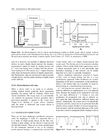
Potentiostat
Working Cathodic Anodic
electrode 0.6
(Si wafer) Reference Counter Passivation potential
Current (mA/cm 2 ) 0.2
electrode electrode 0.4
n-Si p-Si 0 Oxide
Anodic −0.2 free Surface oxide
oxide −0.4 Etching No etching
Pt
Etching solution −0.4 0 0.4 0.8 1.2 1.6
Etch mask
Applied potential (Volts)
(a) (b)
Figure 21.4 (a) Electrochemical cell for silicon electrochemical etching in KOH: p-type silicon etched; n-silicon
passivated by anodic oxide. Reproduced from Wong, S.S. et al. (1992), by permission of Electrochemical Society Inc and
(b) passivation potential and anodic oxidation regime. From Collins, S.C. (1997), by permission of IEEE
stop. It is, however, not possible to fabricate electrical would buckle and a too highly tensile-stressed film
devices on such a highly doped material. For instance, would crack. The film has also to be resistant to alkaline
piezoresistors cannot be made by doping because the etchants. Silicon nitride fulfils both requirements, and it
p ++ etch stop doping level is higher than the piezore- is almost universally used. It is also electrically (and
sistor doping level. The stresses in p ++ doped structures thermally) insulating so that resistors can be readily
make them mechanically inferior to lightly doped mate- deposited on it, and it is optically transparent.
rial. Furthermore, slips are introduced in silicon because Silicon diaphragm fabrication, pictured in Figure
of high stresses, and this makes bonding of highly doped 21.5(b), relies on timed etching, but this is a very
wafers difficult. unsatisfactory approach if thin membranes are needed.
Depending on the device requirement on the membrane,
40 µm is the thinnest that can reasonably be made by
21.4.1 Electrochemical etch stop
timed etching in a manufacturing environment.
p ++ etch stop has two variants: either the p ++ layer is
When a silicon wafer is an anode in an alkaline-
etching solution biased positively above passivation made by diffusion (or implantation) or it is an epitaxial
potential, the surface will be oxidized, which stops layer. Because the doping levels required for etch stop
++
silicon dissolution. The n-type layer of a pn-structure are very high, diffusion p is limited to very thin
can similarly be protected. Positive potential, above membranes. If pn-junction etch stop is utilized, we
passivation potential, is applied to the n-type layer have again the same alternatives: diffusion doping and
(Figure 21.4). Etching of p-type silicon continues epitaxy. Additionally, the n-layer has to be electrically
until the diode is destroyed, and n-type silicon is contacted, and this contact has to be protected from the
then passivated. alkaline silicon etchant. Holders of various designs have
been invented, with the drawback that part of the wafer
front side is used for sealing the holder, leading to silicon
21.5 DIAPHRAGM FABRICATION
There are two basic diaphragm (membrane) structures:
either the diaphragm is made of a deposited film or
it is made of single-crystal silicon. In the first case,
etching is quite simple: all the silicon is removed and
the thin film remains. There are two main considerations
for the membrane material: it has to be (slightly) (a) (b) (c)
tensile-stressed because a compressively stressed film Figure 21.5 Nitride, bulk silicon and SOI diaphragms