
Page 225 - Sami Franssila Introduction to Microfabrication
P. 225
204 Introduction to Microfabrication
5. How much etch non-uniformity can native oxide
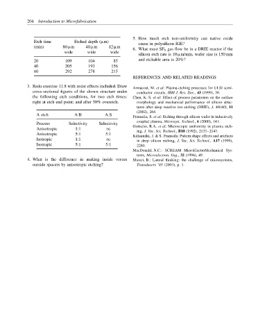
Etch time Etched depth (µm) cause in polysilicon RIE?
(min) 80 µm 40 µm 12 µm 6. What must SF 6 gas flow be in a DRIE reactor if the
wide wide wide
silicon etch rate is 10 µm/min, wafer size is 150 mm
20 109 104 85 and etchable area is 20%?
40 205 193 156
60 292 278 215
REFERENCES AND RELATED READINGS
3. Redo exercise 11.8 with resist effects included. Draw Armacost, M. et al: Plasma-etching processes for ULSI semi-
cross-sectional figures of the shown structure under conductor circuits, IBM J. Res. Dev., 43 (1999), 39.
the following etch conditions, for two etch times: Chen, K.-S. et al: Effect of process parameters on the surface
right at etch end point; and after 50% overetch. morphology and mechanical performance of silicon struc-
tures after deep reactive ion etching (DRIE), J. MEMS, 11
(2002), 264.
A etch A:B A:S
Franssila, S. et al: Etching through silicon wafer in inductively
Process Selectivity Selectivity coupled plasma, Microsyst. Technol., 6 (2000), 141.
Anisotropic 1:1 ∞ Gottscho, R.A. et al: Microscopic uniformity in plasma etch-
ing, J. Vac. Sci. Technol., B10 (1992), 2133–2147.
Anisotropic 5:1 5:1 Kiiham¨ aki, J. & S. Franssila: Pattern shape effects and artefacts
Isotropic 1:1 ∞ in deep silicon etching, J. Vac. Sci. Technol., A17 (1999),
Isotropic 5:1 5:1 2280.
MacDonald, N.C.: SCREAM MicroElectroMechanical Sys-
tems, Microelectron. Eng., 32 (1996), 49.
4. What is the difference in making inside versus Murari, B.: Lateral thinking: the challenge of microsystems,
outside spacers by anisotropic etching? Transducers ’03 (2003), p. 1.