
Page 220 - Sami Franssila Introduction to Microfabrication
P. 220
20
Plasma-etched Structures
Plasma etching is a technology that enables narrow oxide selectively against silicon is a heavily polymer-
linewidths and high aspect ratios. It has completely izing process and selectivity depends on this polymer-
replaced wet etching for feature patterning in modern ization. A three-step oxide etch process consists of a
ICs and it is mandatory in polysilicon surface microme- bulk etching step, an end point step which is highly
chanics. It has also been applied to structures and appli- selective (and polymerizing), followed by a third, low-
cations that are not at all possible with wet etching. For power step that removes polymeric residues: a few extra
instance, plasma etching without resist mask is essential nanometres of silicon are lost in the low-power etch
for planarization and spacer formation. step but wafer cleaning that follows will be much easier
(Figure 20.1).
A combination of anisotropic and isotropic etching
20.1 MULTI-STEP ETCHING
steps can be used to make free-standing structures with
Etching a single layer structure can be accomplished in vertical walls (Figure 20.2). One version is known as
a single step, but multi-step etching can be used for SCREAM (for Single CRystal Etching And Metalliza-
improved process control. In polysilicon gate etching, a tion) and it consists of the following steps:
three-step process is typical:
– anisotropic plasma-etching for the trench (oxide
Step 1: Native oxide breakthrough:
– low oxide selectivity; hard mask);
– a few nanometres of native oxide are – spacer oxide deposition by CVD;
quickly removed in CF 4 /Ar;
– some polysilicon is etched too.
Step 2: Bulk etching:
– optimized for high rate and vertical pro-
file: HCl/HBr.
Step 3: End point and overetch:
– the last 50 nm of poly etched in HCl/HBr;
– high selectivity to oxide.
Note that the underlying oxide loss is a sum of four
different factors:
1. polysilicon film (non)uniformity;
2. polysilicon etch process (non)uniformity;
3. poly:oxide selectivity;
4. overetch time.
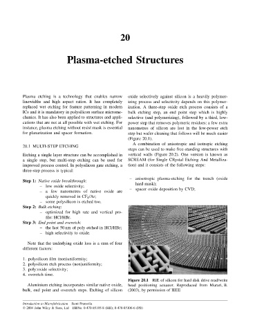
Figure 20.1 RIE of silicon for hard disk drive read/write
Aluminium etching incorporates similar native oxide, head positioning actuator. Reproduced from Murari, B.
bulk, end point and overetch steps. Etching of silicon (2003), by permission of IEEE
Introduction to Microfabrication Sami Franssila
2004 John Wiley & Sons, Ltd ISBNs: 0-470-85105-8 (HB); 0-470-85106-6 (PB)