
Page 216 - Sami Franssila Introduction to Microfabrication
P. 216
Self-aligned Structures 195
cobalt deposition 2000 keV He backscattering yield
◦
annealing in argon to form CoSi at 550 C 10000
9000
cobalt etching 8000
7000
annealing in argon to form CoSi 2 at 650 C. 6000
◦
Yield 5000
4000
The silicide reaction takes place where the metal and 3000
2000
the silicon are in contact, but no reaction takes place on 1000
0
the oxide. However, there is the possibility of bridging: 0 500 1000 1500 2000 2500
some silicon (from either the source/drain area or the Energy
(a)
polysilicon gate) diffuses over the spacer, and the sili-
2000 keV He backscattering yield
cide reaction will then take place there as well. This is 9000
highly undesirable, because S/D/G would then be electri- 8000
7000
cally contacted. Annealing in two steps avoids this: the 6000
first, low-temperature-annealing step, forms monosili- Yield 5000
4000
cide CoSi, which enables selective etching of the unre- 3000
acted cobalt. The second annealing is done to lower the 2000
1000
resistivity of the silicide, and in the case of cobalt, CoSi 2 0
has the lowest resistivity (for nickel, NiSi is the desired 0 500 1000 1500 2000 2500
Energy
final state, and NiSi 2 formation has to be avoided). (b)
The silicide thickness is determined by the metal
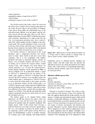
Figure 19.4 RBS spectra of cobalt silicide formation: (a)
thickness, and a compromise between two factors
ca. 30 nm cobalt on silicon and (b) ca. 100 nm CoSi 2 on
must be made: thick silicide would have lower sheet
silicon. Figure courtesy Jaakko Saarilahti, VTT
resistance, but it is not compatible with shallow
junctions and leads to increased leakage currents. In
breakdown, and it is a delicate process. Titanium can
theory, 1 nm of metallic titanium will result in 2.2 nm
reduce oxides, and thin oxide does not prevent the
of silicide, all of it below the original surface. Cobalt
silicidation reaction, but cobalt and nickel do not reduce
silicide, CoSi 2 , will consume even more silicon: the
oxides, and a clean surface is of paramount importance.
silicide thickness is ca. 3.5 times the cobalt thickness.
Titanium salicide presents other novel features, which
Cobalt silicide formation can be measured by RBS, as
are discussed below.
shown in Figure 19.4. In as-deposited sample, a signal
at 1550 keV is obtained from the top surface of the
cobalt, and a signal at 1100 keV is obtained from the Titanium salicide process flow
silicon at the Si/Co interface. In an annealed sample, the
spacer etching
cobalt leading edge is unchanged at 1550 keV because
HF-dip
it comes from the cobalt atoms at the surface, just like titanium deposition
in an as-deposited sample, but the trailing edge is at ◦
annealing in nitrogen to form TiSi 2 and TiN at 750 C
1420 keV because some cobalt atoms have diffused into titanium and TiN etching
the silicon during reaction. Similarly, some silicon atoms annealing to reduce TiSi 2 resistivity.
have diffused to the surface, and the silicon leading edge
signal is at 1150 keV. Note that the area under the cobalt Titanium is annealed in nitrogen. The surface of tita-
signal is unchanged, because no cobalt atoms are lost in nium will react with nitrogen to form TiN, and this TiN
the silicidation process. film will suppress lateral growth of the salicide over the
The surface needs to be cleaned before metal spacers. A simple one-step anneal in argon, which would
deposition. An HF-dip removes the native oxide, but produce a predictable thickness of titanium silicide, is
it will, however, also etch the CVD oxide spacer, and not possible because of excessive lateral growth over the
therefore its duration must be carefully optimized. The spacers. Furnace annealing is not practical because resid-
nitride spacer width would remain intact because a ual oxygen in furnace incorporates into titanium and
LPCVD nitride has very high selectivity against dilute prevents silicidation reaction. Rapid thermal annealing
HF. It is also possible to remove the native oxide in (RTA) equipment is better suited to applications where
the sputtering system by RF sputter etching. However, gas phase impurities must be tightly controlled. Con-
argon ion bombardment is prone to produce damage, trol measurement for the first anneal is the silicide sheet
for example, gate oxide charging and charge-induced resistance. First annealing has to be optimized so that