
Page 221 - Sami Franssila Introduction to Microfabrication
P. 221
200 Introduction to Microfabrication
20.2.1 WSi 2 /polysilicon (polycide) etching
Step 1: WSi 2 etching: Cl 2 /He/O 2 for WSi 2 ;
Step 2: Poly etching: Cl 2 /HBr for poly;
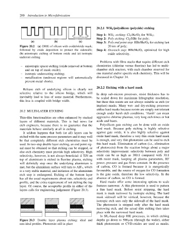
(a) (b) (c) Step 3: Poly end point step: HBr/He/O 2 for etching last
Figure 20.2 (a) DRIE of silicon with oxide/nitride mask; 20 nm of poly;
followed by oxide deposition to protect the sidewalls; Step 4: Overetch step: HBr/He/O 2 optimized for high
(b) anisotropic etching of bottom oxide and (c) isotropic oxide selectivity.
undercut etching
Problems with films stacks that require different etch
– anisotropic spacer etching (oxide removed at bottom chemistries (chlorine versus fluorine) has led to multi-
and on top of mask oxide); chamber etch reactors, with each chamber reserved for
– isotropic undercutting etching; one material and/or specific etch chemistry. This will be
– metallization (undercut regions will automatically discussed in Chapter 34.
prevent metal shorts).
20.2.2 Etching with a hard mask
Release etch of underlying silicon is clearly not
selective relative to the silicon bridge, which will In deep sub-micron processes, resist thickness has to
inevitably lead to loss of some material. Furthermore, be scaled down for maximum lithographic resolution,
this loss is coupled with bridge width. but these thin resists are not always suitable as etch (or
implant) masks. Many wet- and dry-etching processes
utilize hard masks because resists are simply not tolerant
20.2 MULTI-LAYER ETCHING
enough under harsh etch conditions. ‘Harsh’ can mean
Thin-film functionalities are often enhanced by stacked aggressive chlorine plasmas, very long etch times or hot
layers of different materials. This is bad news for acids and bases.
etch engineers, because there is no guarantee that the Polysilicon gate etching can be done with an oxide
materials behave similarly at all in etching. hard mask. Because poly etching is highly selective
It seldom happens that both (or all) layers can be against gate oxide, it is also highly selective against
etched with the same process parameters and it may well oxide hard mask, therefore a very thin oxide hard mask
be that completely different etch chemistries must be is enough, and very thin photoresist can be used to etch
used. In two-step double layer etching, an end point sig- this hard mask. Elimination of carbon (i.e., elimination
nal must be obtained so that etching can be stopped, or of photoresist) from the reaction brings about a major
else etch chemistry must provide high selectivity. High selectivity improvement: selectivity between poly and
selectivity, however, is not always beneficial: if TiN on oxide can be as high as 300:1 compared with 30:1
top of aluminium is etched in fluorine plasma, etching with resist mask, keeping all plasma parameters, RF
will definitely stop once the underlying aluminium is power, pressure and gas flows constant. In the presence
met, but the aluminium surface will turn to AlF 3 , which of carbon, CO is formed because it is energetically
is a very stable material, and initiation of the aluminium favourable, and the source of oxygen for CO formation
etch step is endangered. Etching of the bottom layer is the gate oxide, therefore the low selectivity. In the
has all the usual requirements about rate, selectivity and absence of carbon, no CO is formed.
profile, and the extra requirement of not etching the top Hard masks offer some interesting options to scale
layer. Of course, the acceptable profile in either of the features narrower. A thin photoresist is used to pattern
layers calls for engineering judgement (Figure 20.3). a thin hard mask. Before resist stripping, the hard
mask is made narrower by isotropic etching. The hard
mask sidewall will be vertical, however, because the
isotropic etch sees only the sidewall of the hard mask.
The photoresist is stripped only after the hard mask
narrowing etch, and the actual film etching then takes
place with the narrowed hard mask.
In SF 6 -based deep RIE processes, in which etching
Figure 20.3 Double layer plasma etching: ideal and depths go down to 500 µm (through the wafer), either
non-ideal profiles. Photoresist still in place thick photoresists or CVD-oxides are used as masks.