
Page 226 - Sami Franssila Introduction to Microfabrication
P. 226
21
Wet-etched Silicon Structures
Microsystems technology relies on anisotropic wet
etching of silicon for many major applications. Bulk
micromechanics depends on silicon crystal plane–de-
pendent etching, and many surface micromechanical
and SOI devices make use of silicon wet etching for
auxiliary structures, even though main device features
are defined by plasma etching. Because <100> silicon
is the workhorse of microsystems, the discussion
concentrates on it. Both <110> and <111> etching (a) (b)
will be reviewed briefly.
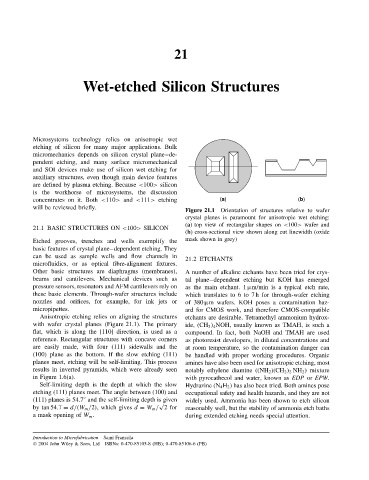
Figure 21.1 Orientation of structures relative to wafer
crystal planes is paramount for anisotropic wet etching:
(a) top view of rectangular shapes on <100> wafer and
21.1 BASIC STRUCTURES ON <100> SILICON
(b) cross-sectional view shown along cut linewidth (oxide
Etched grooves, trenches and wells exemplify the mask shown in grey)
basic features of crystal plane–dependent etching. They
can be used as sample wells and flow channels in
21.2 ETCHANTS
microfluidics, or as optical fibre-alignment fixtures.
Other basic structures are diaphragms (membranes), A number of alkaline etchants have been tried for crys-
beams and cantilevers. Mechanical devices such as tal plane–dependent etching but KOH has emerged
pressure sensors, resonators and AFM cantilevers rely on as the main etchant. 1 µm/min is a typical etch rate,
these basic elements. Through-wafer structures include which translates to 6 to 7 h for through-wafer etching
nozzles and orifices, for example, for ink jets or of 380 µm wafers. KOH poses a contamination haz-
micropipettes. ard for CMOS work, and therefore CMOS-compatible
Anisotropic etching relies on aligning the structures etchants are desirable. Tetramethyl ammonium hydrox-
with wafer crystal planes (Figure 21.1). The primary ide, (CH 3 ) 4 NOH, usually known as TMAH, is such a
flat, which is along the [110] direction, is used as a compound. In fact, both NaOH and TMAH are used
reference. Rectangular structures with concave corners as photoresist developers, in diluted concentrations and
are easily made, with four (111) sidewalls and the at room temperature, so the contamination danger can
(100) plane as the bottom. If the slow etching (111) be handled with proper working procedures. Organic
planes meet, etching will be self-limiting. This process amines have also been used for anisotropic etching, most
results in inverted pyramids, which were already seen notably ethylene diamine ((NH 2 )(CH 2 ) 2 NH 2 ) mixture
in Figure 1.6(a). with pyrocathecol and water, known as EDP or EPW.
Self-limiting depth is the depth at which the slow Hydrazine (N 4 H 2 ) has also been tried. Both amines pose
etching (111) planes meet. The angle between (100) and occupational safety and health hazards, and they are not
(111) planes is 54.7 and the self-limiting depth is given widely used. Ammonia has been shown to etch silicon
◦
√
by tan 54.7 = d/(W m /2), which gives d = W m / 2 for reasonably well, but the stability of ammonia etch baths
a mask opening of W m . during extended etching needs special attention.
Introduction to Microfabrication Sami Franssila
2004 John Wiley & Sons, Ltd ISBNs: 0-470-85105-8 (HB); 0-470-85106-6 (PB)