
Page 227 - Sami Franssila Introduction to Microfabrication
P. 227
206 Introduction to Microfabrication
80 80
µm/h µm/h
60
60
40 40
20 20
(010) (010)
90° 90°
75° (111) + (131) 75°
(111)
60° 60°
45° (111) 45°
30° 30°
0° 15° 0° 15°
(a) (b)
◦
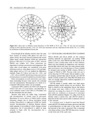
Figure 21.2 Etch rates in different crystal directions in 50% KOH at 78 C: (a) <100> Si: fast, but not maximum
etching in (010) direction and (b) <110> Si: (010) near maximum etch rate. Reproduced from Seidel, H. et al. (1990),
by permission of Electrochemical Society Inc
Even though all the alkaline etchants share the same 21.3 ETCH MASKS AND PROTECTIVE COATINGS
basic features of etching (100) planes fast and (111)
planes slowly, the actual selectivity between the crystal Silicon dioxide and silicon nitride are the common
masking materials for anisotropic wet etching. KOH
planes needs careful attention. KOH has selectivities
etches oxides fast, while TMAH and EDP, hardly at all.
between (100) and (111) of the order of 200:1, whereas
Nitride is more resistant than oxide in both solutions.
TMAH only exhibits 30:1. These selectivities are Mask etch rates depend on temperature and concentra-
dependent on etchant concentration and temperature. But tion just like silicon etch rates, but some general guide-
when other crystal planes are considered, even more lines can be given. An oxide thickness of 2 µm is needed
differences pop up: when planes such as (110) and high-
for through-wafer etching in KOH, whereas 200 nm is
index planes such as (311) are studied, the differences
enough in TMAH or EDP. Thermal oxide etch rate is
multiply. Figure 21.2 shows etch rates for <100> and
slower than that of CVD oxides. Silicon nitride is a bet-
<110> silicon in KOH. Identifying minima and maxima ter masking material than silicon dioxide, and LPCVD
etchrateplanesisessentialforpredictionofetchedshapes. nitride is hardly etched at all, while PECVD nitride etch
Early investigations on etch selectivities were some-
rates are strongly deposition condition dependent, as is
times misleading because wafer miscut will confound
usual with CVD films.
etch rate measurement. Discrepancies of a factor of 2,
LPCVD nitride is usually under very high stress;
compared with present values, are not unusual. gigapascal-range tensile stresses are not atypical. This
Isopropanol (IPA) addition into KOH will change the leads to defects in the underlying silicon, and defects
relative etch rates of crystal planes, and depending on will change etch rates; (100) to (111) crystal plane
exact conditions, either of the (100) or (110) planes will selectivity can change by a factor of 3. For this reason,
be the maximum etch rate planes. pad oxides are employed: as discussed in connection
Because etch times are rather long, evaporation with LOCOS oxidation (Chapter 13), a thin, 10 to 50 nm
and decomposition of etchant must be prevented. thermal oxide is grown first, and LPCVD nitride is
Dissolution of excess silicon in TMAH before etching deposited on this pad oxide in order to eliminate stresses
eliminates changes due to silicon dissolution during to the substrate.
etching. Pyrocathecol is employed in EDP for similar As a practical issue, it should be noted that thermal
reasons: decomposition of ethylene diamine releases oxide and LPCVD nitride are furnace processes and film
small amounts of pyrocathecol, which changes etchant is grown/deposited on both sides of the wafer so that
composition, but if pyrocathecol is added in large the backside of the wafer is protected. This is important
amounts to begin with, the decomposition has a when deep etching is done. PECVD deposition is usually
negligible effect. on the front side of the wafer only.