
Page 223 - Sami Franssila Introduction to Microfabrication
P. 223
202 Introduction to Microfabrication
The planarization wavelength of spin-film is a few
micrometres or tens of micrometres in the lateral
direction. They are thus methods for local planarization
only. Etchback with dummy patterns can provide global
planarization, at the expense of more complex design
and processing.
(a) (b) (c)
Figure 20.7 Trench/plug fill (a) trench etching; (b) thin
liner plus thick conformal (CVD) deposition and (c) etching 20.5 PATTERN SIZE AND PATTERN DENSITY
will result in planar surface (with some plug recess) EFFECTS
the wafer area, but at etching end point the situation 20.5.1 Loading effects
changes dramatically: the plugs may represent only a
few percent of the wafer area, and the etch rate will go Loading effect or area-dependent reaction rate is a
up as all the etch gases attack the tungsten in the plugs. common phenomenon in chemical reactions. For a
process optimized for a certain etchable area, the
flow may not be high enough to supply reactants to
keep the etch rate identical when area is increased
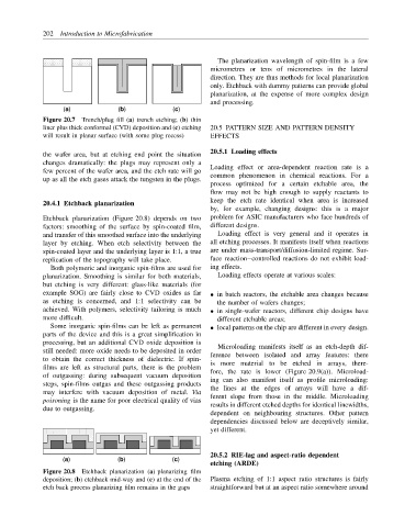
20.4.1 Etchback planarization
by, for example, changing designs: this is a major
Etchback planarization (Figure 20.8) depends on two problem for ASIC manufacturers who face hundreds of
factors: smoothing of the surface by spin-coated film, different designs.
and transfer of this smoothed surface into the underlying Loading effect is very general and it operates in
layer by etching. When etch selectivity between the all etching processes. It manifests itself when reactions
spin-coated layer and the underlying layer is 1:1, a true are under mass-transport/diffusion-limited regime. Sur-
replication of the topography will take place. face reaction–controlled reactions do not exhibit load-
Both polymeric and inorganic spin-films are used for ing effects.
planarization. Smoothing is similar for both materials, Loading effects operate at various scales:
but etching is very different: glass-like materials (for
example SOG) are fairly close to CVD oxides as far • in batch reactors, the etchable area changes because
as etching is concerned, and 1:1 selectivity can be the number of wafers changes;
achieved. With polymers, selectivity tailoring is much • in single-wafer reactors, different chip designs have
more difficult. different etchable areas;
Some inorganic spin-films can be left as permanent • local patterns on the chip are different in every design.
parts of the device and this is a great simplification in
processing, but an additional CVD oxide deposition is
Microloading manifests itself as an etch-depth dif-
still needed: more oxide needs to be deposited in order
ference between isolated and array features: there
to obtain the correct thickness of dielectric. If spin-
films are left as structural parts, there is the problem is more material to be etched in arrays, there-
of outgassing: during subsequent vacuum deposition fore, the rate is lower (Figure 20.9(a)). Microload-
steps, spin-films outgas and these outgassing products ing can also manifest itself as profile microloading:
the lines at the edges of arrays will have a dif-
may interfere with vacuum deposition of metal. Via
poisoning is the name for poor electrical quality of vias ferent slope from those in the middle. Microloading
due to outgassing. results in different etched depths for identical linewidths,
dependent on neighbouring structures. Other pattern
dependencies discussed below are deceptively similar,
yet different.
20.5.2 RIE-lag and aspect-ratio dependent
(a) (b) (c)
etching (ARDE)
Figure 20.8 Etchback planarization (a) planarizing film
deposition; (b) etchback mid-way and (c) at the end of the Plasma etching of 1:1 aspect ratio structures is fairly
etch back process planarizing film remains in the gaps straightforward but at an aspect ratio somewhere around