
Page 224 - Sami Franssila Introduction to Microfabrication
P. 224
Plasma-etched Structures 203
2:1, a phenomenon known as RIE-lag manifests itself: step. For 380 µm wafers, these numbers translate to ca.
smaller features etch slower than larger features. Gas 40 µm, 20 µm and 10 µm trench widths in through-
conductance in deep narrow holes is low and the reac- wafer structures, and holes have even more severe
tants simply cannot reach the bottom effectively (simi- dependency on aspect ratios than long trenches. In
larly, reaction product removal is hindered). RIE-lag is bonded SOI wafers, device layer thicknesses range
not related to RIE-reactors; it is present in all plasma- from 5 µm upwards. Feature size is then limited by
etching systems irrespective of actual reactor design. lithography and undercutting of pulsed (Bosch) process
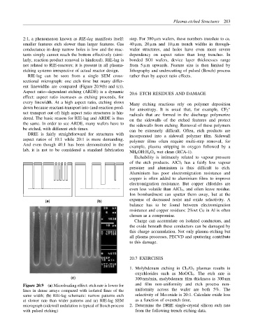
RIE-lag can be seen from a single SEM cross- rather than by aspect ratio effects.
sectional micrograph: one etch time but many differ-
ent linewidths are compared (Figure 20.9(b) and (c)).
Aspect ratio–dependent etching (ARDE) is a dynamic 20.6 ETCH RESIDUES AND DAMAGE
effect: aspect ratio increases as etching proceeds, for
every linewidth. At a high aspect ratio, etching slows Many etching reactions rely on polymer deposition
down because reactant-transport into (and reaction prod- ∗
for anisotropy. It is usual that, for example, CF 2
uct transport out of) high aspect ratio structures is hin- radicals that are formed in the discharge polymerize
dered. The basic reason for RIE-lag and ARDE is thus on the sidewalls of the etched features and protect
the same. In order to see ARDE, many wafers have to the sidewalls from etching. Removal of these polymers
be etched, with different etch times. can be extremely difficult. Often, etch products are
DRIE is fairly straightforward for structures with incorporated into a sidewall polymer film. Sidewall
aspect ratios of 10:1 while 20:1 is more demanding. polymer films often require multi-step removal, for
And even though 40:1 has been demonstrated in the example, plasma stripping in oxygen followed by a
lab, it is not to be considered a standard fabrication
NH 4 OH:H 2 O 2 wet clean (RCA-1).
Etchability is intimately related to vapour pressure
of the etch products. AlCl 3 has a fairly low vapour
pressure and aluminium is thus difficult to etch.
Aluminium has poor electromigration resistance and
copper is often added to aluminium films to improve
electromigration resistance. But copper chlorides are
even less volatile than AlCl 3 , and often leave residue.
Ion bombardment can sputter them away, but at the
expense of decreased resist and oxide selectivity. A
(a) (b)
balance has to be found between electromigration
resistance and copper residues: 2%wt Cu in Al is often
chosen as a compromise.
Charge can accumulate on isolated conductors, and
the oxide beneath these conductors can be damaged by
this charge accumulation. Not only plasma etching but
all plasma processes, PECVD and sputtering contribute
to this damage.
20.7 EXERCISES
1. Molybdenum etching in Cl 2 /O 2 plasmas results in
oxychlorides such as MoOCl 4 . The etch rate is
(c) 300 nm/min, molybdenum film thickness is 300 nm
Figure 20.9 (a) Microloading effect: etch rate is lower for and film non-uniformity and etch process non-
lines in dense arrays compared with isolated lines of the uniformity across the wafer are both 5%. The
same width; (b) RIE-lag schematic: narrow patterns etch selectivity of Mo:oxide is 20:1. Calculate oxide loss
at slower rate than wider patterns and (c) RIE-lag SEM as a function of overetch time.
micrograph (sidewall undulation is typical of Bosch process 2. Determine the DRIE single-crystal silicon etch rate
with pulsed etching) from the following trench etching data.