
Page 222 - Sami Franssila Introduction to Microfabrication
P. 222
Plasma-etched Structures 201
DRIE processes that use Cl 2 chemistry use metals such
as chromium or nickel as etch masks. Etching of thick
oxide structures (>10 µm) (for optical waveguides or
capillary electrophoresis channels) uses thick polysili-
con, amorphous silicon or metal masks.
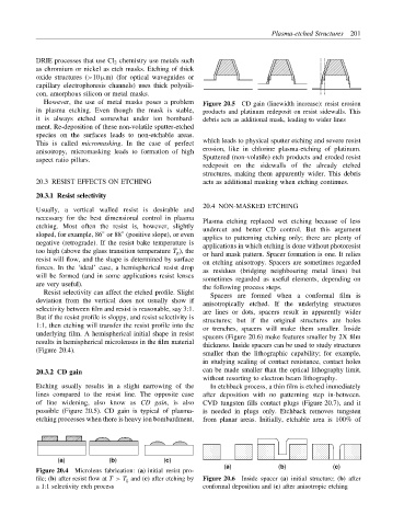
However, the use of metal masks poses a problem Figure 20.5 CD gain (linewidth increase): resist erosion
in plasma etching. Even though the mask is stable, products and platinum redeposit on resist sidewalls. This
it is always etched somewhat under ion bombard- debris acts as additional mask, leading to wider lines
ment. Re-deposition of these non-volatile sputter-etched
species on the surfaces leads to non-etchable areas.
This is called micromasking. In the case of perfect which leads to physical sputter etching and severe resist
anisotropy, micromasking leads to formation of high erosion, like in chlorine plasma-etching of platinum.
Sputtered (non-volatile) etch products and eroded resist
aspect ratio pillars.
redeposit on the sidewalls of the already etched
structures, making them apparently wider. This debris
20.3 RESIST EFFECTS ON ETCHING acts as additional masking when etching continues.
20.3.1 Resist selectivity
20.4 NON-MASKED ETCHING
Usually, a vertical walled resist is desirable and
necessary for the best dimensional control in plasma
Plasma etching replaced wet etching because of less
etching. Most often the resist is, however, slightly undercut and better CD control. But this argument
◦
◦
sloped, for example, 86 or 88 (positive slope), or even
applies to patterning etching only; there are plenty of
negative (retrograde). If the resist bake temperature is applications in which etching is done without photoresist
too high (above the glass transition temperature T g ), the or hard mask pattern. Spacer formation is one. It relies
resist will flow, and the shape is determined by surface on etching anisotropy. Spacers are sometimes regarded
forces. In the ‘ideal’ case, a hemispherical resist drop as residues (bridging neighbouring metal lines) but
will be formed (and in some applications resist lenses sometimes regarded as useful elements, depending on
are very useful). the following process steps.
Resist selectivity can affect the etched profile. Slight Spacers are formed when a conformal film is
deviation from the vertical does not usually show if anisotropically etched. If the underlying structures
selectivity between film and resist is reasonable, say 3:1. are lines or dots, spacers result in apparently wider
But if the resist profile is sloppy, and resist selectivity is structures; but if the original structures are holes
1:1, then etching will transfer the resist profile into the or trenches, spacers will make them smaller. Inside
underlying film. A hemispherical initial shape in resist spacers (Figure 20.6) make features smaller by 2X film
results in hemispherical microlenses in the film material
thickness. Inside spacers can be used to study structures
(Figure 20.4).
smaller than the lithographic capability; for example,
in studying scaling of contact resistance, contact holes
20.3.2 CD gain can be made smaller than the optical lithography limit,
without resorting to electron beam lithography.
Etching usually results in a slight narrowing of the In etchback process, a thin film is etched immediately
lines compared to the resist line. The opposite case after deposition with no patterning step in-between.
of line widening, also know as CD gain, is also CVD tungsten fills contact plugs (Figure 20.7), and it
possible (Figure 20.5). CD gain is typical of plasma- is needed in plugs only. Etchback removes tungsten
etching processes when there is heavy ion bombardment, from planar areas. Initially, etchable area is 100% of
(a) (b) (c)
(a) (b) (c)
Figure 20.4 Microlens fabrication: (a) initial resist pro-
file; (b) after resist flow at T > T g and (c) after etching by Figure 20.6 Inside spacer (a) initial structure; (b) after
a 1:1 selectivity etch process conformal deposition and (c) after anisotropic etching