
Page 232 - Sami Franssila Introduction to Microfabrication
P. 232
Wet-etched Silicon Structures 211
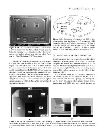
{111}
<100> {111} {100} {100}
<010>
<011>
{110}
<001> {110}
Figure 21.11 Orientation of structures on (100) wafer.
◦
Alignment to wafer flat leads to 54.7 angles and {111}
sidewalls. Alignment 45 relative to flat leads to {110} walls
◦
and {100} vertical walls result when rates of {110} relative
Figure 21.10 Bulk silicon micromachined accelerometer: to {100} fulfil Conditions 21.1 and 21.2. Reproduced from
a 380 µm thick wafer has been etched through: concave Powell, O. & H. Harrison (2001), by permission of IOP
holes show familiar <111> limited sidewalls, but at convex
corners fast etching planes have been revealed. Photo
courtesy Risto Mutikainen, VTI Technologies 21.7 FRONT SIDE BULK MICROMACHINING
Cantilevers and bridges can be made by front side micro-
Simulation of anisotropic wet etching has been around machining by undercutting. Either convex corners are
for years but until recently it has not had a major designed into release etch openings (Figure 21.14), or
impact. New simulation tools such as MICROCAD can else the structures are aligned not to main axes of sili-
◦
take into account most of the crystal plane effects and con, but for example 45 off, so that fast etching planes
double side etching as well. MICROCAD is a geometric appear. This method was used to make the silicon bridge
simulator based on experimentally determined etch in Figure 2.1(b).
rates of crystal planes. The alternative is the atomistic All structures made on the bridges, membranes
approach: bond directions, bond breakage and bond or cantilevers have to be processed before the sil-
energies are analysed. Atomistic simulators can explain icon release etch because topology and topography
surface roughness, which is beyond the capabilities of do not allow lithography after release. Piezoresistors,
geometric simulators. thermopiles and AFM tips are typical devices on
(100)
(111) (111)
(110)
(101) (101) 90°
(100)
50 µm
−10 µm −10 µm
(a) (b)
◦
◦
Figure 21.12 (a) 45 slanted sidewalls in <100> wafer by 45 degree off-orientation. Reproduced from Strandman, C.
et al. (1995), by permission of IEEE and (b) 90 angles in <100> wafer, before and after etch-mask removal. Note the
◦
severe undercut that is unavoidable to make vertical walls in <100>. From Vazsonyi, E. et al. (2003), by permission of
IOP