
Page 233 - Sami Franssila Introduction to Microfabrication
P. 233
212 Introduction to Microfabrication
This is possible with a little extra effort in mask
design by adding compensation structures, shown in
Figure 21.15.
The fast etching planes start to erode at convex
corners. But the final convex corner is protected by
this sacrificial structure so that after the compensation
structure has been etched away, a rectangular corner
remains.
Timing is the difficult part: if etching is stopped
too early, a peak remains on the corner. Overetching
leads to a structure with an undercut corner, similar to
the non-compensated case but with less undercut. Even
though this method looks perfect in two dimensions, it
leaves some small <311> surfaces in three dimensions,
as seen in Figure 21.8. Another shortcoming of this
method is that it takes a lot of space to form these
compensation structures.
Figure 21.13 Etching through <100> silicon from two 21.9 <110> ETCHING
sides simultaneously. Reproduced from Nijdam, A.J. et al.
(1999), by permission of IOP Silicon of <110> orientation offers an interesting possi-
bility to anisotropically wet etch perfectly vertical walls
cantilevers. Structures already made, resistors, junc- when the mask is aligned so that slow-etching (111)
tions, tips, have to be covered during silicon etch- planes form the sidewalls (Figure 21.16). However, just
ing, but because etch times are short compared to as in the case of <100> silicon etching, the relative rates
backside through-wafer etching, CVD oxide films of of different crystal planes can be changed by etchant
standard thickness (<1 µm) can be used as protec- concentration and temperature. It is possible to find con-
tive coatings. ditions in which square bottom profile can be achieved,
for instance, KOH (23% wt)-H 2 O-isopropanol (10–15%
◦
◦
wt) at 85 C or 30% KOH at 70 C.
21.8 CORNER COMPENSATION Under other etch conditions (for instance with 40%
KOH at 70 C), a self-limiting shape, U-groove, is met
◦
We noted in Section 21.6 that convex corners are (Figure 21.17). U-grooves are self-limiting just like V-
dominated by (311) planes (Figure 21.8). In many grooves on (100) wafers, when planes that etch slower
designs, it would be very useful to have sharp corners. than (110) appear. Etching will proceed until the six
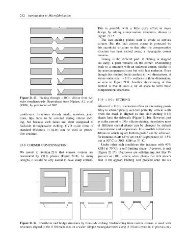
Figure 21.14 Cantilever and bridge structures by front-side etching. Underetching from convex corners is used, with
structures aligned to the [110] main axes on a wafer. Simple rectangular holes along [110] axis result in V-grooves only