
Page 234 - Sami Franssila Introduction to Microfabrication
P. 234
Wet-etched Silicon Structures 213
(a) (b)
Figure 21.15 (a) Different designs for corner compensation. Figure courtesy Ville Voipio, Helsinki University
of Technology and (b) optical microscope image of a compensated corner after etching. Photo courtesy Seppo
Marttila, Helsinki University of Technology
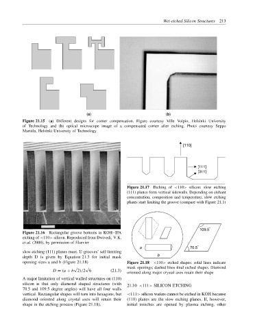
[110]
[111]
[311]
Figure 21.17 Etching of <110> silicon: slow etching
(111) planes form vertical sidewalls. Depending on etchant
concentration, composition and temperature, slow etching
planes start limiting the groove (compare with Figure 21.1)
109.5 °
Figure 21.16 Rectangular groove bottoms in KOH–IPA
etching of <110> silicon. Reproduced from Dwivedi, V.K.
et al. (2000), by permission of Elsevier
a 70.5 °
slow etching (111) planes meet. U-grooves’ self-limiting
depth D is given by Equation 21.3 for initial mask b
opening sizes a and b (Figure 21.18) Figure 21.18 <110> etched shapes: solid lines indicate
√ √ mask openings; dashed lines final etched shapes. Diamond
D = (a + b 2)/2 6 (21.3)
oriented along major crystal axes retain their shape
A major limitation of vertical walled structures on (110)
silicon is that only diamond shaped structures (with 21.10 <111> SILICON ETCHING
70.5 and 109.5 degree angles) will have all four walls
vertical. Rectangular shapes will turn into hexagons, but <111> silicon wafers cannot be etched in KOH because
diamond oriented along crystal axes will retain their (111) planes are the slow etching planes. If, however,
shape in the etching process (Figure 21.18). initial trenches are opened by plasma etching, other