
Page 239 - Sami Franssila Introduction to Microfabrication
P. 239
218 Introduction to Microfabrication
Table 22.1 Materials for released structures
Structural film Sacrificial film(s) Technology/application
Polysilicon CVD oxide, PSG Surface micromechanics
Silicon nitride CVD oxide Thermal isolation
Electroplated nickel Cu, resist LIGA
Al Resist, PECVD oxide Post-CMOS processing
Au Cu, resist Air bridges in RF circuits
Parylene Resist Microfluidics
SU-8 Cu, Al Microfluidics
Cu Resist Post-CMOS processing
10 µm span lengths (for electroplated gold) to centime- mirrors and as inductor coils with minimized substrate
tres (for silicon nitride) are possible for released lat- capacitance, among others.
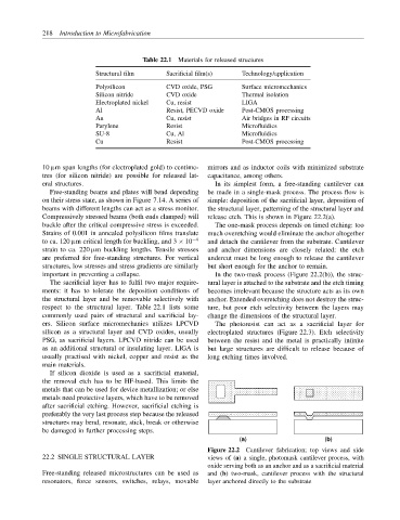
eral structures. In its simplest form, a free-standing cantilever can
Free-standing beams and plates will bend depending be made in a single-mask process. The process flow is
on their stress state, as shown in Figure 7.14. A series of simple: deposition of the sacrificial layer, deposition of
beams with different lengths can act as a stress monitor. the structural layer, patterning of the structural layer and
Compressively stressed beams (both ends clamped) will release etch. This is shown in Figure 22.2(a).
buckle after the critical compressive stress is exceeded. The one-mask process depends on timed etching: too
Strains of 0.001 in annealed polysilicon films translate much overetching would eliminate the anchor altogether
to ca. 120 µm critical length for buckling, and 3 × 10 −4 and detach the cantilever from the substrate. Cantilever
strain to ca. 220 µm buckling lengths. Tensile stresses and anchor dimensions are closely related: the etch
are preferred for free-standing structures. For vertical undercut must be long enough to release the cantilever
structures, low stresses and stress gradients are similarly but short enough for the anchor to remain.
important in preventing a collapse. In the two-mask process (Figure 22.2(b)), the struc-
The sacrificial layer has to fulfil two major require- tural layer is attached to the substrate and the etch timing
ments: it has to tolerate the deposition conditions of becomes irrelevant because the structure acts as its own
the structural layer and be removable selectively with anchor. Extended overetching does not destroy the struc-
respect to the structural layer. Table 22.1 lists some ture, but poor etch selectivity between the layers may
commonly used pairs of structural and sacrificial lay- change the dimensions of the structural layer.
ers. Silicon surface micromechanics utilizes LPCVD The photoresist can act as a sacrificial layer for
silicon as a structural layer and CVD oxides, usually electroplated structures (Figure 22.3). Etch selectivity
PSG, as sacrificial layers. LPCVD nitride can be used between the resist and the metal is practically infinite
as an additional structural or insulating layer. LIGA is but large structures are difficult to release because of
usually practised with nickel, copper and resist as the long etching times involved.
main materials.
If silicon dioxide is used as a sacrificial material,
the removal etch has to be HF-based. This limits the
metals that can be used for device metallization; or else
metals need protective layers, which have to be removed
after sacrificial etching. However, sacrificial etching is
preferably the very last process step because the released
structures may bend, resonate, stick, break or otherwise
be damaged in further processing steps.
(a) (b)
Figure 22.2 Cantilever fabrication; top views and side
22.2 SINGLE STRUCTURAL LAYER views of (a) a single, photomask cantilever process, with
oxide serving both as an anchor and as a sacrificial material
Free-standing released microstructures can be used as and (b) two-mask, cantilever process with the structural
resonators, force sensors, switches, relays, movable layer anchored directly to the substrate