
Page 214 - Sami Franssila Introduction to Microfabrication
P. 214
19
Self-aligned Structures
Lithography is most often discussed as a resolution
question: how small a structure can be printed on the
wafer? Alignment is equally important: how closely can
the structures on the different mask levels be aligned
with each other? Device-packing density is clearly
dependent on both.
Self-alignment is a process by which two struc-
tures are aligned to each other non-lithographically.
The existing structures act as masks for subsequent
steps. Unlike photoresist, these structures are fixed and
are integral parts of the device. Self-alignment offers
inherently accurate alignment between two structures
because alignment is not determined by the optome-
chanical lithography tool but by the structures and mate-
rials themselves.
In this chapter, the examples are related to CMOS but
self-alignment is not limited to CMOS: it can be applied
widely in microdevice fabrication. More examples
will be presented in chapters on sacrificial structures
(Figure 22.11), bipolar technology (Figure 26.3), pro-
cessing on non-silicon substrates (Figure 29.3) and
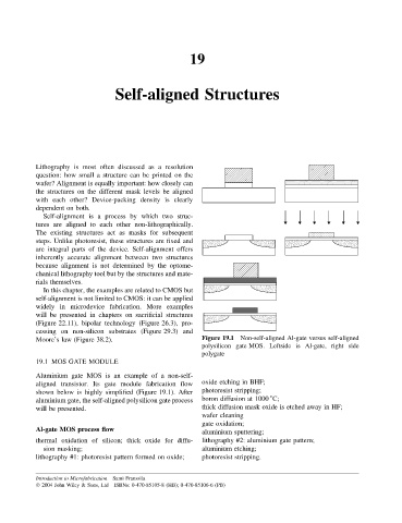
Moore’s law (Figure 38.2). Figure 19.1 Non-self-aligned Al-gate versus self-aligned
polysilicon gate MOS. Leftside is Al-gate, right side
polygate
19.1 MOS GATE MODULE
Aluminium gate MOS is an example of a non-self-
aligned transistor. Its gate module fabrication flow oxide etching in BHF;
shown below is highly simplified (Figure 19.1). After photoresist stripping;
◦
aluminium gate, the self-aligned polysilicon gate process boron diffusion at 1000 C;
will be presented. thick diffusion mask oxide is etched away in HF;
wafer cleaning
gate oxidation;
Al-gate MOS process flow aluminium sputtering;
thermal oxidation of silicon; thick oxide for diffu- lithography #2: aluminium gate pattern;
sion masking; aluminium etching;
lithography #1: photoresist pattern formed on oxide; photoresist stripping.
Introduction to Microfabrication Sami Franssila
2004 John Wiley & Sons, Ltd ISBNs: 0-470-85105-8 (HB); 0-470-85106-6 (PB)