
Page 210 - Sami Franssila Introduction to Microfabrication
P. 210
Moulding and Stamping 189
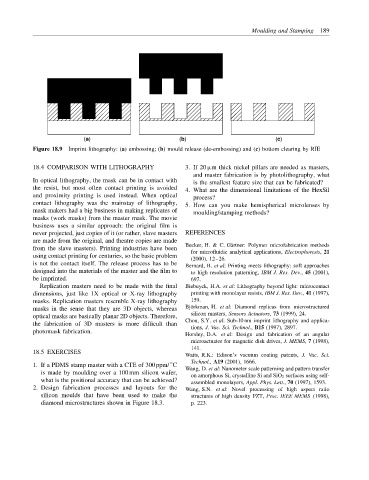
(a) (b) (c)
Figure 18.9 Imprint lithography: (a) embossing; (b) mould release (de-embossing) and (c) bottom clearing by RIE
18.4 COMPARISON WITH LITHOGRAPHY 3. If 20 µm thick nickel pillars are needed as masters,
and master fabrication is by photolithography, what
In optical lithography, the mask can be in contact with is the smallest feature size that can be fabricated?
the resist, but most often contact printing is avoided 4. What are the dimensional limitations of the HexSil
and proximity printing is used instead. When optical process?
contact lithography was the mainstay of lithography, 5. How can you make hemispherical microlenses by
mask makers had a big business in making replicates of moulding/stamping methods?
masks (work masks) from the master mask. The movie
business uses a similar approach: the original film is
never projected, just copies of it (or rather, slave masters REFERENCES
are made from the original, and theatre copies are made
from the slave masters). Printing industries have been Becker, H. & C. G¨ artner: Polymer microfabrication methods
for microfluidic analytical applications, Electrophoresis, 21
using contact printing for centuries, so the basic problem (2000), 12–26.
is not the contact itself. The release process has to be Bernard, B. et al: Printing meets lithography: soft approaches
designed into the materials of the master and the film to to high resolution patterning, IBM J. Res. Dev., 45 (2001),
be imprinted. 697.
Replication masters need to be made with the final Biebuyck, H.A. et al: Lithography beyond light: microcontact
dimensions, just like 1X optical or X-ray lithography printing with monolayer resists, IBM J. Res. Dev., 41 (1997),
masks. Replication masters resemble X-ray lithography 159.
masks in the sense that they are 3D objects, whereas Bj¨ orkman, H. et al: Diamond replicas from microstructured
optical masks are basically planar 2D objects. Therefore, silicon masters, Sensors Actuators, 73 (1999), 24.
the fabrication of 3D masters is more difficult than Chou, S.Y. et al: Sub-10 nm imprint lithography and applica-
tions, J. Vac. Sci. Technol., B15 (1997), 2897.
photomask fabrication.
Horsley, D.A. et al: Design and fabrication of an angular
microactuator for magnetic disk drives, J. MEMS, 7 (1998),
141.
18.5 EXERCISES
Waits, R.K.: Edison’s vacuum coating patents, J. Vac. Sci.
Technol., A19 (2001), 1666.
◦
1. If a PDMS stamp master with a CTE of 300 ppm/ C
Wang, D. et al: Nanometer scale patterning and pattern transfer
is made by moulding over a 100 mm silicon wafer,
on amorphous Si, crystalline Si and SiO 2 surfaces using self-
what is the positional accuracy that can be achieved? assembled monolayers, Appl. Phys. Lett., 70 (1997), 1593.
2. Design fabrication processes and layouts for the Wang, S.N. et al: Novel processing of high aspect ratio
silicon moulds that have been used to make the structures of high density PZT, Proc. IEEE MEMS (1998),
diamond microstructures shown in Figure 18.3. p. 223.