
Page 208 - Sami Franssila Introduction to Microfabrication
P. 208
Moulding and Stamping 187
a round object can be rolled over a PDMS stamp and
a spiral structure created. Microcoils have been made
in this way. Alternatively, the PDMS piece can be
curved and used as a mould. Polyurethane moulded
into a curved PDMS results in a curved, rigid piece of
(a) (b) polyurethane.
Figure 18.6 (a) sagging of low AR structures and (b)
lateral collapse of high AR structures
18.3 3D-VOLUME STAMPING
problematic. Structures with ca. 1:1 aspect ratios and Volume stamps are rigid. Silicon wafers make excellent
uniform pattern densities, such as periodic structures, stamp masters: they combine thermal and mechanical
are less problematic than structures with either very low stability with the possibility of fabricating elaborate
or very high aspect ratios, or a mix of different aspect shapes with good surface finish. Electroplated metals
ratios or pattern densities (Figure 18.6). are also widely used stamp materials.
◦
Polymers are stamped at temperatures 5 to 100 C
above their glass transition temperatures, which trans-
18.2.1 Microcontact printing (µCP) lates to 50 to 200 C. Both the stamp surface and the
◦
sidewalls make intimate contact with the polymer. The
Microcontact printing is a microlithographic version of 3D nature of the rigid stamp is of paramount impor-
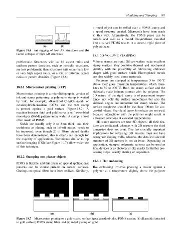
ink-and-stamp patterning: a polymeric stamp is wetted tance: not only the surface smoothness but also the
by ‘ink’, for example, alkanethiol CH 3 (CH 2 ) 15 SH or
sidewall angles are important for stamp release. The
octadecyltrichlorosilane (OTS), and the wet stamp
surface roughness should be less than 100 nm for suc-
is pressed against a gold surface (Figure 18.7). A
cessful release. Sacrificial layers for release are not used,
reaction between thiol and gold leaves a self-assembled
because interactions with the polymer might result in
monolayer (SAM) pattern on the wafer. A stamp is most
unwanted reactions at elevated temperatures.
often made of PDMS.
3D stamp masters are true 3D objects: all their fea-
SAMs are usually only 2 to 3 nm thick, and their tures are replicated, whereas with 2D masters the third
usefulness as plating, etch or lift-off masks, needs to dimension does not print. This has crucially important
be improved; even though 20 to 30 nm etched depths implications for releasing: 3D masters must not have
have been demonstrated, this is clearly not enough for retrograde sloping walls, whereas, the detailed sidewall
the majority of applications. Techniques similar to top structure of 2D masters is not an issue. Depending on
surface imaging (TSI) (see Figure 10.7) allow wider use application, stamped polymeric patterns can be used as
of this technique.
final devices or as photoresist-like masks for further pro-
cessing steps, usually etching or deposition.
18.2.2 Stamping non-planar objects
18.3.1 Hot embossing
PDMS is flexible, and this opens up special applications:
patterns can be contact-printed on curved surfaces. Hot embossing involves pressing a master against a
Gratings on optical fibers have been realized. Similarly, polymer at a temperature slightly above the polymer
(a) (b) (c)
Figure 18.7 Microcontact printing on a gold-coated surface: (a) alkanethiol-inked PDMS master; (b) alkanethiol attached
to gold surface; PDMS stamp lifted and (c) metal plating on gold