
Page 209 - Sami Franssila Introduction to Microfabrication
P. 209
188 Introduction to Microfabrication
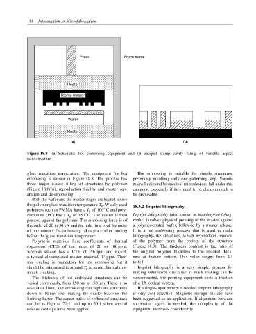
Press Force frame
Heater
Stamp master
Wafer
Heater
(a) (b)
Figure 18.8 (a) Schematic hot embossing equipment and (b) unequal stamp cavity filling of variable aspect
ratio structure
glass transition temperature. The equipment for hot Hot embossing is suitable for simple structures,
embossing is shown in Figure 18.8. The process has preferably involving only one patterning step. Various
three major issues: filling of structures by polymer microfluidic and biomedical microdevices fall under this
(Figure 18.8(b)), reproduction fidelity and master sep- category, especially if they need to be cheap enough to
aration and de-embossing. be disposable.
Both the wafer and the master stages are heated above
the polymer glass transition temperature T g . Widely used 18.3.2 Imprint lithography
◦
polymers such as PMMA have a T g of 106 C and poly-
◦
carbonate (PC) has a T g of 150 C. The master is then Imprint lithography (also known as nanoimprint lithog-
pressed against the polymer. The embossing force is of raphy) involves physical pressing of the master against
the order of 20 to 30 kN and the hold time is of the order a polymer-coated wafer, followed by a master release.
of one minute. De-embossing takes place after cooling It is a hot embossing process that is used to make
below the glass transition temperature. lithography-like structures, which necessitates removal
Polymeric materials have coefficients of thermal of the polymer from the bottom of the structure
expansion (CTE) of the order of 20 to 100 ppm, (Figure 18.9). The thickness contrast is the ratio of
whereas silicon has a CTE of 2.6 ppm and nickel, the original polymer thickness to the residual thick-
a typical electroplated master material, 13 ppm. Ther- ness at feature bottom. This value ranges from 2:1
mal cycling is mandatory for hot embossing but it to 6:1.
should be minimized to around T g to avoid thermal mis- Imprint lithography is a very simple process for
match cracking. making submicron structures: if mask making can be
The thickness of hot embossed structures can be subcontracted, the printing equipment costs a fraction
varied enormously, from 150 nm to 150 µm. There is no of a 1X optical system.
resolution limit, and embossing can replicate structures If a single-layer pattern is needed, imprint lithography
down to 10 nm size; making the master becomes the is very cost effective. Magnetic storage devices have
limiting factor. The aspect ratios of embossed structures been suggested as an application. If alignment between
can be as high as 20:1, and up to 50:1 when special successive layers is needed, the complexity of the
release coatings have been applied. equipment increases considerably.