
Page 207 - Sami Franssila Introduction to Microfabrication
P. 207
186 Introduction to Microfabrication
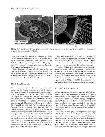
Stator Parallel plates
Rotor
Anchored column
(a) (b)
Figure 18.5 HexSil moulded and released polysilicon pieces attached to a carrier wafer. Reproduced from Horsley, D.A.
et al. (1998), by permission of IEEE
parts, and the rest of the wafer is etched away. In a sense, Poly dimethylsiloxane is a favourite material for
the wafer itself is a sacrificial mould. The process begins many microdevice applications because it is chemically
by standard etching and doping steps, and ends up with inert, transparent down to 250 nm and flexible. PDMS
KOH/TMAH etching. Owing to mechanical fragility of is used in microchannels and microreactors, and it is
thin p ++ structures, bonding to glass or to another wafer widely used as the master for 2D-surface stamping.
is often done before dissolution. Because PDMS is a polymeric material, its processing
When the mould will is completely removed, freedom does not necessitate elevated temperatures, and a variety
of shape is unlimited. If the material to be moulded can of materials can be used as moulds. PDMS pre-polymer
fill retrograde features, these pose no problem in release. is poured over the mould, and cured, for example, at
◦
With reusable moulds, retrograde shapes are not allowed 80 C for 10 h. PDMS will demould easily because of its
because the mould has to be released. inertness. However, because of its coefficient of thermal
◦
expansion of ca. 300 ppm/ C, PDMS is not suitable for
applications that require accurate pattern positioning.
18.1.2 Reusable moulds
Silicon wafers with etched structures, electroplated 18.2 2D SURFACE STAMPING
metals and SU-8 epoxy structures are typical materials
for reusable moulds. The release process must damage Surface stamps are soft, elastic materials, like polymer
neither the mould nor the moulded piece. This can PDMS. These stamps conform to surfaces, but detach
be helped by a couple of methods: the mould can easily and retain their shape even after intimate contact.
be coated with a material that eliminates reactions Both elastic constant and surface energy are important
between the materials, or an anti-stiction surface coating considerations for soft stamps. Stiffer materials offer
can be applied. Diamond would be a good choice higher resolution but worse contact. Hybrid stamps
for a mould for both the above-mentioned reasons. with a stiff mechanical backing and a soft stamping
Several Teflon-like fluoropolymer coatings, such as surface have been devised in order to have the best of
deposition from CHF 3 or C 4 F 8 gases in a plasma and both worlds.
vacuum desiccator treatment with tridecafluoro-1,1,2,2- The contact area plays an important role: light
tetrahydrooctyl-1trichlorosilane, have also been utilized. field structures, with a small contact area, are non-
Another way to go is to deposit a sacrificial layer on problematic because separation force is small. Structures
the mould master and release the structures by etching. with aspect ratios not too far from unity and structures
The mould can be reused after another sacrificial layer with fairly uniform pattern densities, such as periodic
deposition. The HexSil process (Figure 18.4 and 18.5) structures, are less prolematic than if the aspect ratios
makes use of a CVD oxide–release layer and a LPCVD of structures to be stamped differ from unity or
polysilicon as the structural material. from each other considerably, when stamping becomes