
Page 202 - Sami Franssila Introduction to Microfabrication
P. 202
Bonding and Layer Transfer 181
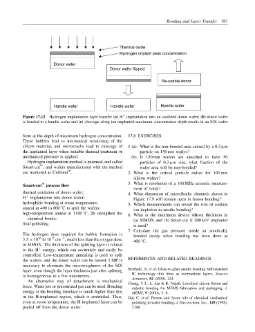
Thermal oxide
Hydrogen implant peak concentration
Donor wafer
Donor wafer flipped
Re-usable donor
Handle wafer Handle wafer Handle wafer
+
Figure 17.12 Hydrogen implantation layer transfer (a) H implantation into an oxidized donor wafer; (b) donor wafer
is bonded to a handle wafer and (c) cleavage along ion implanted maximum concentration depth results in an SOI wafer
form at the depth of maximum hydrogen concentration. 17.8 EXERCISES
These bubbles lead to mechanical weakening of the
silicon material, and microcracks lead to cleavage of 1 (a). What is the non-bonded area caused by a 0.3 µm
the implanted layer when suitable thermal treatment or particle on 150 mm wafers?
mechanical pressure is applied. (b). If 150 mm wafers are specified to have 50
Hydrogen implantation method is patented, and called particles of 0.3 µm size, what fraction of the
Smart-cut , and wafers manufactured with the method wafer area will be non-bonded?
are marketed as Unibond . 2. What is the critical particle radius for 100 mm
silicon wafers?
Smart-cut process flow 3. What is resolution of a 160 MHz acoustic measure-
ment of voids?
thermal oxidation of donor wafer; 4. What dimension of microfluidic channels shown in
+
H implantation into donor wafer; Figure 17.9 will remain open in fusion bonding?
hydrophilic bonding at room temperature; 5. Which measurements can reveal the role of sodium
anneal at 400 to 600 C to split the wafers; ion depletion in anodic bonding?
◦
◦
high-temperature anneal at 1100 C, 2h strengthen the 6. What is the maximum device silicon thickness in
chemical bonds; (a) SIMOX and (b) Smart-cut if 200 keV implanter
final polishing.
is used?
7. Calculate the gas pressure inside an anodically
The hydrogen dose required for bubble formation is bonded cavity when bonding has been done at
17
16
−2
3.5 × 10 to 10 cm , much less than the oxygen dose 400 C.
◦
in SIMOX. The thickness of the splitting layer is related
to the H + energy, which can accurately and easily be
controlled. Low-temperature annealing is used to split
the wafers, and the donor wafer can be reused. CMP is REFERENCES AND RELATED READINGS
necessary to eliminate the microroughness of the SOI
layer, even though the layer thickness just after splitting Berthold, A. et al: Glass-to-glass anodic bonding with standard
is homogeneous to a few nanometres. IC technology thin films as intermediate layers, Sensors
Actuators, 82 (2000), 224.
An alternative way of detachment is mechanical
Cheng, Y.T., L. Lin & K. Najafi: Localized silicon fusion and
force. Water jets or pressurized gas can be used. Bonding
eutectic bonding for MEMS fabrication and packaging, J.
energy at the bonding interface is much higher than that MEMS, 9 (2000), 3–8.
in the H-implanted region, which is embrittled. Thus, Gui, C. et al: Present and future role of chemical mechanical
even at room temperature, the H-implanted layer can be polishing in wafer bonding, J. Electrochem. Soc., 145 (1998),
peeled off from the donor wafer. 2198.