
Page 199 - Sami Franssila Introduction to Microfabrication
P. 199
178 Introduction to Microfabrication
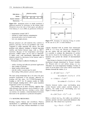
reflective coating
Bulk silicon 2h t
Nitride
Spacer material
Electronics
2R
Figure 17.8 Aluminium mirror on nitride membrane is
addressed pixelwise by electronics in the bottom wafer.
Photoresist serves the roles of both spacer and adhesive.
From Sakarya, S. et al. (2002), by permission of Elsevier 2h
– temperatures around 100 C
◦
– tolerant to (some) particle contamination
– structured wafers can be bonded easily 2R
– low cost, simple process.
Figure 17.9 Geometry for analysing closing of cavities
Because polymers are soft materials they conform to for the case 2h ≪ 2R. t is wafer thickness
particles, and there will be less problems with voids,
compared to stiffer materials like silicon. The main
concept, measured with an atomic force microscope
problem with adhesive bonding is limited long-term
◦
stability and limited thermal range, with ca. 400 C AFM at a 5 × 5 µm site. Because of non-idealities,
the two wafers will not touch fully (Figure 17.9).
maximum. Because of low temperatures and benign
It is possible to estimate the dimensions of cavities
processes, CMOS wafers can be used as substrates.
that can be closed in the bonding process. The same
A mirror array with individually addressable pixel
elements steered by electronics in the bottom wafer is equations also govern the closure of micromachined
shown in Figure 17.8. cavities.
Prototypical steps in adhesive bonding are Gap closing is a function of wafer thickness (t), wafer
mechanical strength determined by Young’s modulus
(E), Poisson ratio (ν) and surface energy (γ ) (ca.
– surface cleaning and adhesion promoter application 2
– spin coating of polymer 100 mJ/m for room temperature bonding). Cavities of
– initial curing (solvent bake) radius R (in the plane of the wafer) will be closed if the
– join the wafers (vacuum may be used) distance between the wafers, h, is
– final curing of the polymer: pressure and/or heat. 2 3 2 1/2
h < R /(2Et /3γ (1 − ν ))
The final curing temperature has to be above the glass for cavities R > 2t, R ≫ h (17.5)
transition temperature of the polymer, otherwise no 2 1/2
bonding will take place. For CYTOP-fluoropolymer h < 3.5(Rγ (1 − ν )/E)
bonding at 160 C for 30 minutes results in 4 MPa for cavities R < 2t, R ≫ h (17.6)
◦
bond strength; bonding below 108 C glass transition
◦
temperature results in no bonding. Particles between wafers cause non-bonding areas
Chip bonding can be done similarly: capping chips (voids) because wafers cannot conform abruptly to
with polymeric ring structures can be bonded to a sub- particles. The radius of the non-bonding area (see
strate in a flip-chip–like way, creating a cavity, which Figure 17.10(a)) is given by
can enclose, for example, a micromechanical resonator
that needs to be operated in a protected atmosphere. 3 2 1/4 √
R = (2Et /3γ (1 – ν )) × h (17.7)
Below a critical size h crit , the wafers can conform to
17.4 BONDING MECHANICS
particles, and the void size is practically identical to the
Bonding requires flatness and smoothness. Flatness particle size. This critical size is given by
specification is a global/large area concept measured
2
over chip or wafer area, whereas smoothness is a local h crit = 5(tγ (1 − ν )/E) 1/2 (17.8)