
Page 200 - Sami Franssila Introduction to Microfabrication
P. 200
Bonding and Layer Transfer 179
the grooves. Higher bonding voltage and temperature
will result in better sealing.
2h
We have seen that silicon fusion bonding reaction
products are hydrogen in the case of hydrophobic
R bonding and water in hydrophilic bonding. If there are
cavities on the wafers, these gases will be trapped in the
cavities. When the temperature is increased, hydrogen
t and water behave differently: hydrogen dissolves into
silicon but water oxidizes silicon. Other gases found in
cavities are probably desorption products from wafer
surfaces, and not trapped during bonding in gaseous
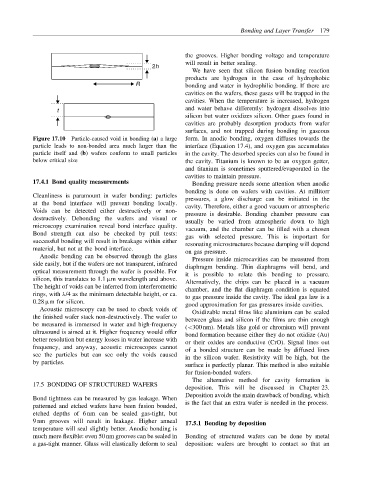
Figure 17.10 Particle-caused void in bonding (a) a large form. In anodic bonding, oxygen diffuses towards the
particle leads to non-bonded area much larger than the interface (Equation 17.4), and oxygen gas accumulates
particle itself and (b) wafers conform to small particles in the cavity. The desorbed species can also be found in
below critical size the cavity. Titanium is known to be an oxygen getter,
and titanium is sometimes sputtered/evaporated in the
cavities to maintain pressure.
17.4.1 Bond quality measurements Bonding pressure needs some attention when anodic
bonding is done on wafers with cavities. At millitorr
Cleanliness is paramount in wafer bonding: particles pressures, a glow discharge can be initiated in the
at the bond interface will prevent bonding locally. cavity. Therefore, either a good vacuum or atmospheric
Voids can be detected either destructively or non- pressure is desirable. Bonding chamber pressure can
destructively. Debonding the wafers and visual or usually be varied from atmospheric down to high
microscopy examination reveal bond interface quality. vacuum, and the chamber can be filled with a chosen
Bond strength can also be checked by pull tests: gas with selected pressure. This is important for
successful bonding will result in breakage within either resonating microstructures because damping will depend
material, but not at the bond interface. on gas pressure.
Anodic bonding can be observed through the glass Pressure inside microcavities can be measured from
side easily, but if the wafers are not transparent, infrared diaphragm bending. Thin diaphragms will bend, and
optical measurement through the wafer is possible. For it is possible to relate this bending to pressure.
silicon, this translates to 1.1 µm wavelength and above.
Alternatively, the chips can be placed in a vacuum
The height of voids can be inferred from interferometric
chamber, and the flat diaphragm condition is equated
rings, with λ/4 as the minimum detectable height, or ca. to gas pressure inside the cavity. The ideal gas law is a
0.28 µm for silicon.
good approximation for gas pressures inside cavities.
Acoustic microscopy can be used to check voids of
Oxidizable metal films like aluminium can be sealed
the finished wafer stack non-destructively. The wafer to
between glass and silicon if the films are thin enough
be measured is immersed in water and high-frequency
(<300 nm). Metals like gold or chromium will prevent
ultrasound is aimed at it. Higher frequency would offer
bond formation because either they do not oxidize (Au)
better resolution but energy losses in water increase with
or their oxides are conductive (CrO). Signal lines out
frequency, and anyway, acoustic microscopes cannot
of a bonded structure can be made by diffused lines
see the particles but can see only the voids caused
in the silicon wafer. Resistivity will be high, but the
by particles.
surface is perfectly planar. This method is also suitable
for fusion-bonded wafers.
The alternative method for cavity formation is
17.5 BONDING OF STRUCTURED WAFERS
deposition. This will be discussed in Chapter 23.
Deposition avoids the main drawback of bonding, which
Bond tightness can be measured by gas leakage. When
patterned and etched wafers have been fusion bonded, is the fact that an extra wafer is needed in the process.
etched depths of 6 nm can be sealed gas-tight, but
9 nm grooves will result in leakage. Higher anneal 17.5.1 Bonding by deposition
temperature will seal slightly better. Anodic bonding is
much more flexible: even 50 nm grooves can be sealed in Bonding of structured wafers can be done by metal
a gas-tight manner. Glass will elastically deform to seal deposition: wafers are brought to contact so that an