
Page 201 - Sami Franssila Introduction to Microfabrication
P. 201
180 Introduction to Microfabrication
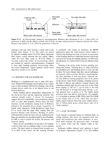
Deposited Top wafer (thinned)
Capping wafer metal
cavity
Adhesive
Base wafer
metallization
Base wafer with devices Base wafer with devices
Figure 17.11 (a) Microriveting: joining by electrodeposition. Redrawn after Shivkumar, B. & C.-J. Kim (1997), by
permission of IEEE and (b) adhesive joining with W-CVD via plugs making electrical connection between the wafers.
Redrawn after Ramm, P. et al. (1997), by permission of Elsevier
opening in the top wafer matches a metal pad on the is symmetric with respect to interfaces. In MEMS
bottom wafer (Figure 17.11). The wafers are joined applications where the oxide between silicon wafers is
by adhesive bonding before W-CVD. Metal deposition etched away during processing, symmetry or asymmetry
then creates contact between the two wafers. Multi- of the bonding interface is important because etch fronts
wafer ICs have been made by W-CVD filling of can travel fast along the bonding interface. In SOI wafer
vias that connect the wafers. In microriveting, wafers specifications, it is stated which wafer has thermal oxide
are bonded by selective electrodeposition. Compared on it.
to most other bonding methods, microriveting offers Thinning of the device wafer involves grinding, pol-
the lowest temperature. Liquid tightness before metal ishing and etching. Thinning down to 10 µm thickness
deposition remains to be clarified. is reasonably easy, and thinning down to 5 µm can also
be done. For layers thinner than this, special techniques
are required: either real time–thickness monitoring dur-
17.6 BONDING FOR SOI WAFER FAB ing final polishing or etch-stop layers. Epitaxial lay-
ers with different etching properties have to be grown
on the device wafer before bonding. Grinding removes
Bonding is a straightforward way to make SOI struc-
tures. Bonded SOI technique uses bonding of two wafers the bulk of silicon, and selective etching removes the
(one or both oxidized) followed by thinning. One of the remaining material until the etch-stop layer is met. High
−3
20
bonded silicon wafers has to be thinned down to the boron doping (≥ 10 cm ) can be used as the etch
desired thickness. stop but because of its high dislocation density, a sec-
Wafer bonding allows independent optimization of ond epitaxial layer is grown on it. The highly doped
the top device layer and the supporting substrate. The etch-stop layer can then be removed by, for example,
substrate (handle wafer), is chosen for mechanical 1–3–8 etchant (a mixture of HF, HNO 3 and CH 3 COOH
in the volume ratio of 1:3:8), which does not etch a
support, thermal compatibility, micromachining, doping
lightly doped material. Etch-stop layers enable fabrica-
level or some other property. Device layer can have
tion of 100 nm thick device silicon layers with ±5 to
material, crystal orientation, doping level or thickness
10 nm variation.
tailored to the particular device design, irrespective of
handle wafer properties. Oxide thicknesses range from
0.3 to 4 µm, with the upper limit coming from the
17.7 LAYER TRANSFER
practical thermal oxide thickness. Bonding of wafers
with deposited oxides has been actively studied, but the Layer transfer is practised along two different lines: in
films are generally not smooth enough for good bonding. cutting methods, thin layers are separated from sub-
If CMP is used to polish the surface, the process cost strates and transferred onto other substrates; in sacri-
increases rapidly. ficial wafer methods, the processed wafer is bonded
There are two possibilities for the pair to be bonded: to a carrier wafer and the original wafer is dis-
a silicon wafer and an oxidized wafer, or two oxidized solved.
wafers. The latter results in reduced bond strength, just Hydrogen bubble–induced layer splitting is based
70 to 80% of the former, but the resulting structure on hydrogen implantation (Figure 17.12). Gas bubbles